
Displays

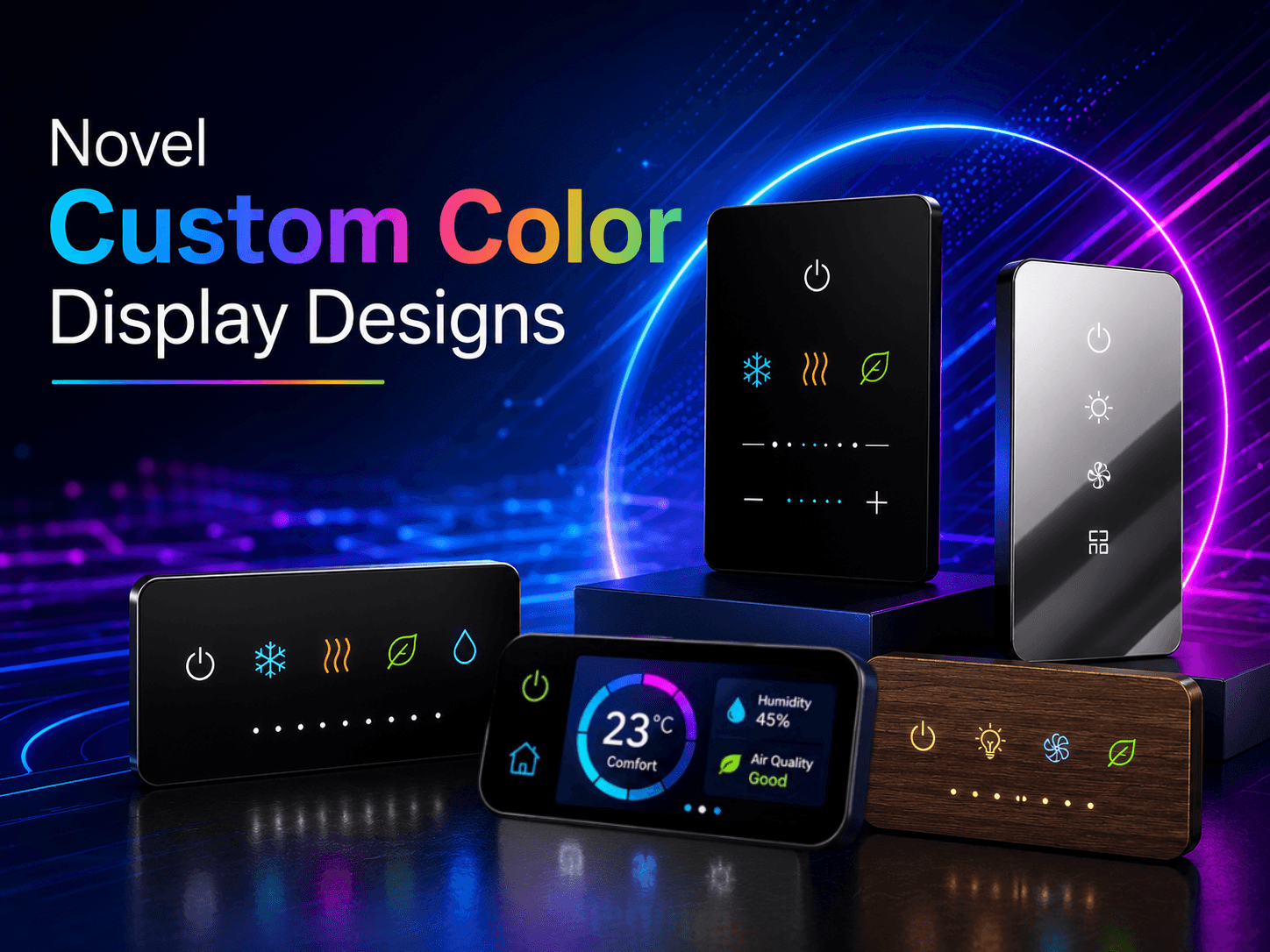
Novel Custom Color Display Designs

Designers often envision color displays that can be created in any shape or size to perfectly match their product aesthetics. In reality, however, display designs are typically constrained by standard TFT or OLED panel sizes.

Customizing a TFT or OLED display can be prohibitively expensive due to high non-recurring engineering (NRE) costs. For example, developing a custom display at Gen 5 TFT production line can require an investment of approximately $300,000 to $400,000. In addition, development cycles are long and generally only feasible for high-volume projects.

To address these challenges, the engineering team at Orient Display has explored innovative approaches to enable more flexible and visually appealing display designs. These concepts have proven highly useful for designers seeking customization without the cost of fully custom panels. Most of these solutions are based on dead-front (all-black) display designs, which offer both aesthetic and functional advantages.


What is a Dead-Front Display?

A dead-front display is a user interface panel that appears completely uniform, such as black, matte black, white, silver, mirror-like, or even wood-textured. When turned off. In this state, all icons, text, and graphics are fully hidden, creating a seamless and minimalist surface.

When the display is illuminated by a backlight, the hidden elements become visible. This creates a clean, high-end, and modern visual effect, making dead-front displays especially popular in applications such as automotive dashboards, smart home appliances, and control panels.

From left to right: Black Dead Front Display, White Silver Dead Front Display, Mirror Dead Front Display


Wood Texture Dead Front Display


If in-house visual assets are limited, the Google Nest design team provides excellent examples of well-integrated display aesthetics, as shown below.


We will further explore black dead-front display concepts in the following design approaches.

Design 1:  Limited Colors With Fixed-Position Color Displays

For products that require simplicity, clarity, and cost efficiency, this approach delivers elegant results.

By using screen printing to define up to three colors in fixed positions, designers can create clean, intuitive interfaces with strong visual contrast. When the display is off, the surface remains perfectly uniform; when illuminated, only the intended elements appear—crisp and refined.

Why it works:

  • Cost-effective solution for mass production
  • High reliability and stable color performance
  • Ideal for appliances, industrial controls, and minimalistic UI designs


Design 2: Unlimited or Gradient Colors with Fixed-Position Color Displays

When your product demands richer visuals or a more premium feel, this approach removes the limitations of traditional color printing.

Instead of relying on screen printing, color films laminated onto the polarizer enable vibrant, multi-color or gradient effects with superior consistency. This allows designers to create visually striking interfaces that stand out in competitive markets.

To ensure optimal visual quality, we recommend maintaining at least 2 mm spacing between color segments to prevent crosstalk.

Why it stands out:

  • Enables unlimited or gradient color designs
  • Delivers a more premium, high-end appearance
  • Ideal for smart home devices, consumer electronics, and branded UI experiences


Design 3: Hybrid Fixed-Position Color Displays with TFT or AMOLED

For the most advanced applications, hybrid designs combine the best of both worlds—static elegance and dynamic intelligence.

By integrating fixed-position color elements with TFT or AMOLED displays, designers can create interfaces that are both visually distinctive and functionally powerful.

Static icons, branding elements, or color zones remain crisp and consistent, while dynamic display areas provide rich content, animation, and interactivity.

What this unlocks:

  • Premium, futuristic product designs
  • Seamless integration of static and dynamic UI elements
  • Maximum design freedom without full custom panel costs

Structure of the Hybrid Passive LCD and Active TFT/AMOLED Display


From Concept to Reality

Great product design is no longer limited by standard display formats. With the right approach, you can achieve custom-looking designs without custom-level cost and risk.

At Orient Display, our engineering team works closely with customers to turn design concepts into manufacturable, high-performance display solutions.

Let’s build something distinctive together.

If you have questions or would like to explore your next design, please contact our engineering.

author-avatar

About Bill Cheung

Senior Engineer

Displays

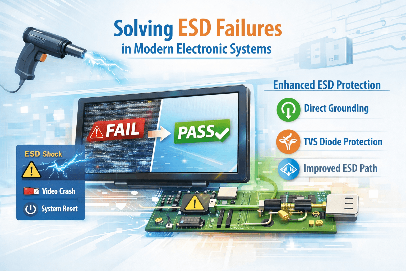
Solving ESD Failures in Modern Electronic Systems

Case Overview – Improving ESD Reliability in large size USB Display System

The exiting display system was upgraded from an older LVDS design to a new USB‑based architecture. During certification testing, the system passed the 8 kV contact discharge test but failed the 15 kV air discharge test. This caused video interruptions and system resets, preventing the product from being approved.

Our engineering team analyzed the issue and identified two main causes:

  1. The USB ground path had too much resistance during an ESD event.
  2. The USB power line did not have strong enough protection against voltage spikes.

After making targeted improvements, the system able to successfully pass the 15 kV air discharge test.

What Was Happening?

During testing, an ESD gun applies a high‑voltage static shock to the outside of the device. This simulates real‑world situations such as a user touching the screen after walking on carpet.

This shock caused the USB interface to momentarily fail, which led to:

  • Video freezing
  • Display blackouts
  • Touch panel communication loss
  • System resets

This happened because the USB interface is more sensitive to static electricity than the older LVDS design.


Root Cause Debug

  1. Grounding Was Too Weak for ESD

The USB ports used ferrite beads between the connector and ground. Ferrite beads are good for filtering noise, but they block fast, high‑energy ESD pulses. This prevented the static charge from safely going to ground.

  1. The USB Power Line Needed Better Protection

The USB 5 V line did not have a fast‑acting protection device to absorb sudden voltage spikes caused by ESD.


What We Changed

To fix the issue, we made four improvements:

✔ Direct Grounding

We removed the ferrite beads (L15 and L20) and connected the USB ground directly to the system ground.
This gives static electricity a clean, low‑resistance path to escape.

✔ Added TVS Protection

We added a high‑speed TVS diode (SP1326‑01LTG) to the USB 5 V line.
This device instantly clamps voltage spikes and protects the USB controller.

✔ Improved ESD Path

The new grounding and protection layout ensures that ESD energy is safely diverted away from sensitive components.

Figure 1


Figure 2


How the Improved Design Works

Before Fix

ESD Shock → Ferrite Bead → Blocked → USB Chip Overloaded → Video Failure

After Fix

ESD Shock → Direct Ground → TVS Clamp → USB Chip Protected → System Stable

Results

After applying these improvements:

  • The system passed 15 kV air discharge
  • No video dropouts or resets occurred
  • USB communication remained stable
  • The product is now ready for certification, BINGO!!

Conclusion

The ESD failures were caused by grounding impedance and insufficient surge protection in the USB interface. By optimizing the ground path and adding proper TVS protection, we restored the system’s reliability and ensured it meets certification requirements.

If you have any questions, please contact our engineering.

author-avatar

About Lily Liang

Account Manager - Orient Display

Displays

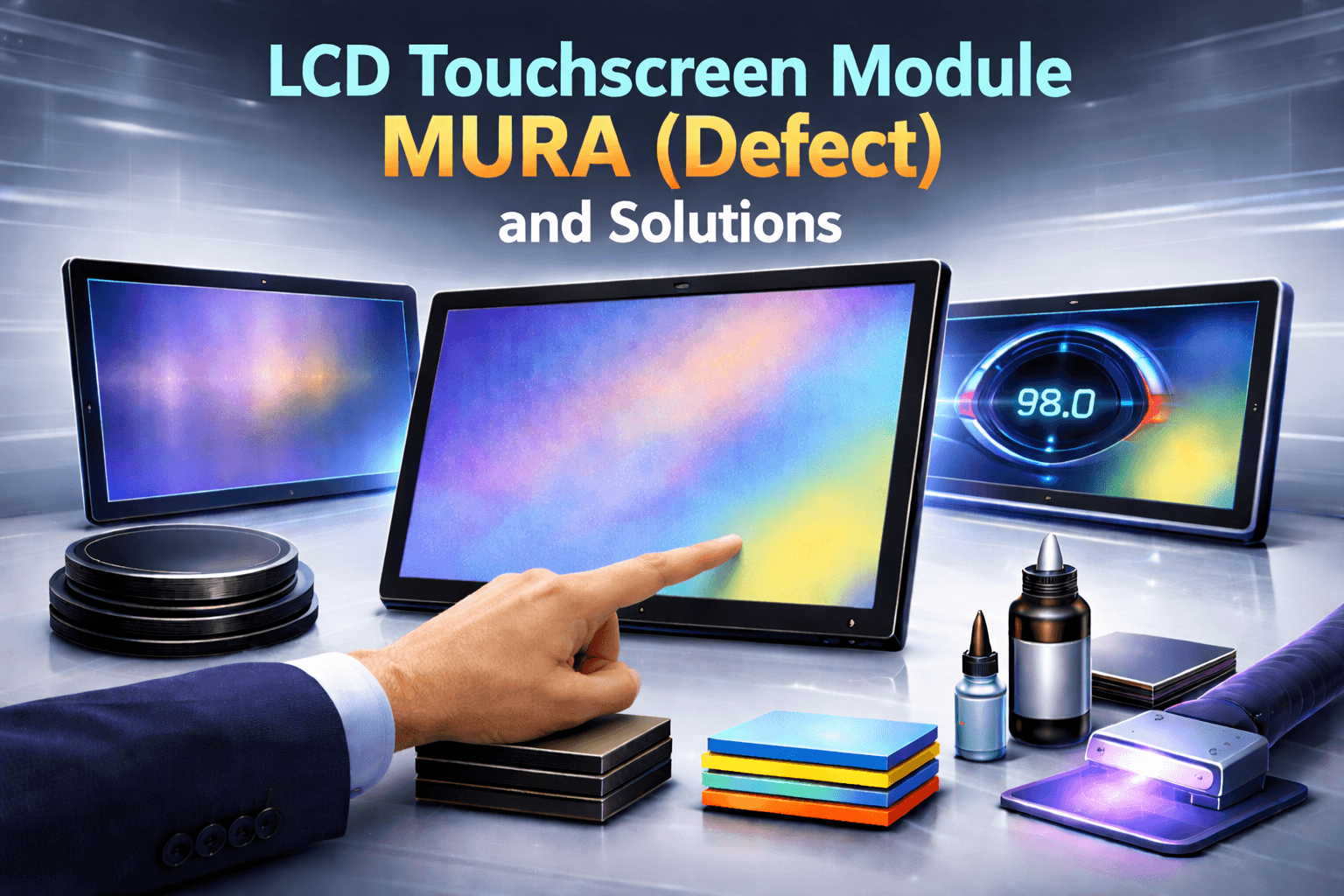
LCD Touchscreen Module Mura (Defect) and Solutions

What is Mura?

“Mura” is the Romanized spelling of the Japanese kanji “斑” (むら), which originally means unevenness, inconsistency, or defects. Because Japan was an early leader in the LCD industry, “Mura” has become a widely used technical term. It refers to various visible artifacts caused by non-uniform brightness in display panels (LCD/OLED).

This issue can occur in televisions, smartphones, and automotive dashboards. Brightness non-uniformity (Mura) affects the viewing experience, reduces the perceived premium quality of a product, and may even interfere with display performance or functionality.

In the context of optical bonding for displays, some manufacturers interpret Mura as light leakage. Since this defect may appear as yellow spots or yellowish lines along the edges on a white screen, many manufacturers also refer to Mura as “yellowing.”


Mura Evaluation (Identification Method)

The simplest way to identify Mura is to switch the display to black, white, or low gray-level images in a dark room. By visually inspecting the edges around the active area (AA), one may observe irregular colors such as white, yellow, or other uneven patterns.

Observing the display from different angles will reveal various types of Mura phenomena, including stripes, patches, and clustered patterns, with no consistent color or shape. If pressure is intentionally applied to the display area, the existing Mura will intensify, and even after removing the external force, the Mura will not disappear immediately.

From the working principle of liquid crystal displays, Mura is essentially unavoidable whenever stress is applied to the liquid crystal cell—it can only vary in severity.

Based on the principle of camera lens filters, Fujifilm developed ND (Neutral Density) filters. These filters come in eight levels: 1%, 2%, 3%, 4%, 5%, 6%, 8%, and 10%. In the industry, Mura is typically classified and evaluated according to these levels.


Neutral Density (ND) Filters

In ND filters, a 1% transmittance filter (ND100 or higher) is more “stringent” (i.e., has stronger light reduction capability) than an 8% transmittance filter (typically ND8 or ND12).

The lower the transmittance percentage of an ND filter, the less light it allows through, meaning it blocks more light and is therefore considered more “intense” or “stronger.”

Specific Comparison:

  • 1% transmittance (approximately ND100–ND1000 or higher):
    Belongs to strong ND filters, reducing light by more than 6–10 stops. Suitable for daytime long-exposure photography, such as capturing flowing water with a silky effect.
  • 8% transmittance (typically ND8–ND12):
    Belongs to weak ND filters, reducing light by about 3 stops. Suitable for shooting in cloudy conditions or at dusk, with relatively mild light reduction.

In summary: The lower the transmittance percentage, the higher the ND value, and the stronger the light reduction capability.


Causes of Mura

Mura can originate from materials or processes in the front-end manufacturing of the display panel (PANEL), though the specific solutions for those are not discussed here. It can also result from materials and processes used during the back-end assembly stages.

This article focuses only on Mura that occurs after optical bonding. Under the assumption that defects in the cover glass, panel, polarizer, backlight, and other materials have been ruled out, the discussion centers on Mura caused by deformation of the liquid crystal cell due to bonding-induced stress.

Typical examples include yellow spots and non-uniform display effects commonly observed after bonding.

Failure Analysis of Defective Units:  A detailed teardown analysis was conducted on defective units. Removing the housing showed no change, and removing the backlight also produced no change. However, after separating the CTP (capacitive touch panel) and TFT, the yellow spots disappeared. When the CTP was reattached and left to rest for several days, the yellow spots reappeared.

This confirms that the Mura defect in this case is related to the bonding materials or processes. In full-lamination processes—whether using OCA (optically clear adhesive) or liquid adhesive—Mura that appears after curing or after a period of rest is strongly related to adhesive selection and curing conditions.

Impact of Optical Adhesive:   First, considering the effect of optical adhesive: polymer-based adhesives tend to be relatively rigid. If the selected thickness is insufficient, their ability to absorb strain is poor. As a result, deformation stress affects the liquid crystal layer, transmitting mechanical distortion to the display. This leads to non-uniformity in the liquid crystal cell gap, causing uneven light transmittance and ultimately resulting in visible color non-uniformity—i.e., Mura.


Solutions for Mura

  • Increase adhesive thickness

    A thicker adhesive layer can absorb more deformation stress. However, this will increase material costs, potentially even doubling them. Therefore, it is not recommended to use OCA with a thickness of 175 μm or thinner.

  • Reduce cover glass thickness

    Thinning the cover glass can help reduce deformation. However, this may also decrease impact resistance and durability.

  • Use softer adhesive (lower elastic modulus)

    Selecting a softer adhesive can help better absorb stress. However, if the adhesive is too soft, it may become difficult to handle during the bonding process.

  • Use laminated (multi-layer) structural adhesive

    This type of adhesive combines the advantages of both thicker adhesive layers and improved stress absorption. It offers the best improvement effect. A schematic diagram of stress distribution after bonding can illustrate this advantage.

Single Layer OCA                                                    Sandwich OCA

  • Reduce bonding pressure appropriately

    Minimize lamination pressure where possible, opt for backlight assembly after bonding, and ensure the bonding platform is as flat as possible. This helps reduce excessive compression and potential damage to the liquid crystal cell.

  • Improve shrinkage behavior of liquid adhesives

    Select materials with lower curing shrinkage. In addition to changing adhesive materials, curing process parameters can also be optimized—for example, using low-intensity, longer-duration UV curing or gradual temperature ramp-up curing. These methods can help mitigate Mura to some extent.


If you have any questions, please contact our engineering.

Displays

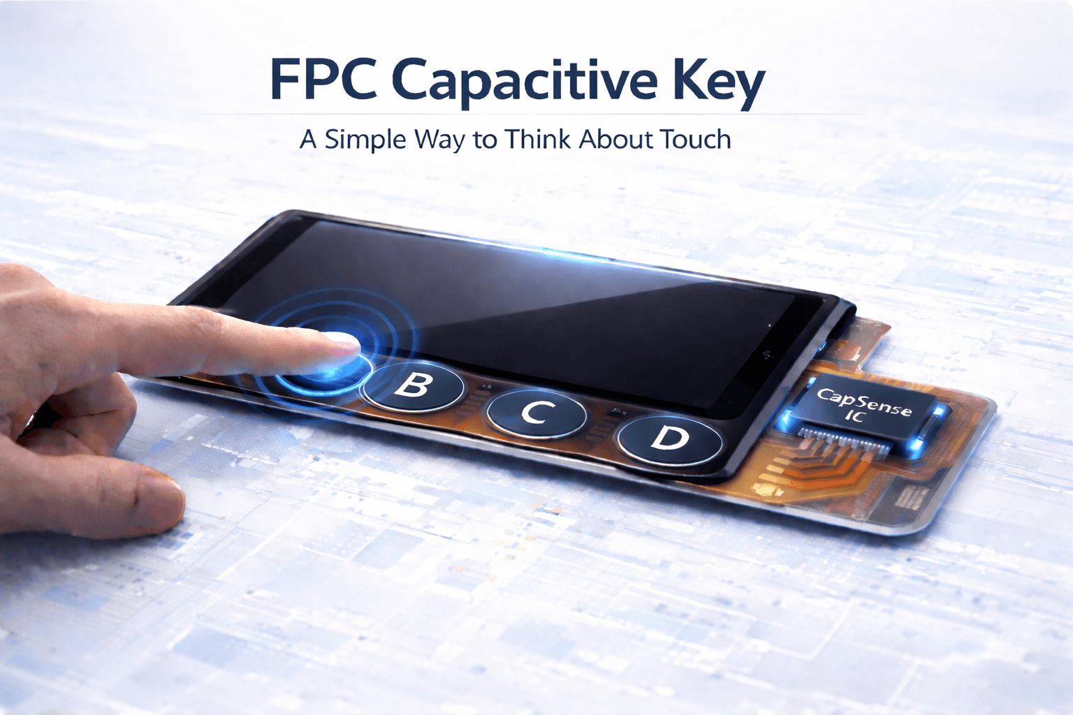
FPC Capacitive Key: A Simple Way to Think About Touch

Sometimes when I look at the touch solutions we use every day, I get the feeling that a lot of designs exist simply because “that’s how it’s usually done,” not because they’re the only option.

Take touch screens, for example.

In most cases, when we say “touch,” we immediately think of a full capacitive touch panel—an entire surface that responds to input anywhere. It works, it’s intuitive, and for many applications, it’s absolutely the right choice.

But when the interaction is limited to just a few buttons, that kind of solution can feel a bit… heavy.


Not All Touch Needs Coordinates

The most common structure we deal with looks something like this:

Cover Lens + OCA + ITO Glass + FPC + Touch Controller

Its job is straightforward: detect where you touch (X-Y coordinates)

This makes perfect sense for interfaces that involve gestures, swiping, or dynamic UI, but not every interaction needs location tracking. Sometimes, all you really need is a simple “trigger.”


A Different Approach: CapSense

This is where capacitive sensing (CapSense) comes in. Instead of tracking position, it detects whether a specific area is being touched.

Typical structure:

Cover Lens + ITO Key (single layer) + FPC + CapSense IC

It’s commonly used for:

  • Buttons
  • Sliders
  • Fixed touch zones

Compared to full touch panels, it simplifies things—but it still relies on ITO.


Taking It One Step Further: Removing ITO

And then there’s an even simpler approach.

FPC Capacitive Key is based on a very straightforward idea:

Replace ITO electrodes with copper electrodes on FPC

Which brings the structure down to:

Cover Lens + FPC + CapSense IC

No ITO layer, no full touch stack. Just what’s necessary.


What It Actually Looks Like

Below is a simplified layout that helps visualize how this approach is implemented.

The display sits in the center; Capacitive keys are distributed around the edges; All key electrodes are routed through the FPC; Each key (A/B/C/D) corresponds to an independent sensing area.

What’s interesting here is that the display and touch inputs are no longer part of the same stack. They coexist—but remain structurally independent.


How It Works

There’s no mechanical action involved, and nothing visibly moves.

  1. Metal electrodes (copper or silver) are formed on the FPC
  2. A sensing IC continuously monitors capacitance
  3. A finger approaches → capacitance changes
  4. The IC detects it and outputs a signal

It feels less like “pressing a button” and more like being detected.


Structurally, It’s Very Simple

From a hardware perspective, the simplicity stands out:

  • Substrate: PET or PI (typically 0.1–0.3 mm)
  • Electrodes: flexible in shape (round, bar, custom)
  • Connection: direct FPC to mainboard
  • Surface: glass or plastic overlay

And one key difference: No need for full ITO film or ITO glass. That alone can open up room in both design and cost.


Manufacturing Is Fairly Straightforward

Typical approaches include:

  • Etching copper electrodes directly on FPC
  • Printing conductive paste (silver or copper)
  • Laminating a protective cover (glass or plastic)
  • Connecting via standard FPC connectors

It feels closer to circuit design than display module integration.


What Stands Out in Practice

After working with this approach, a few characteristics become quite noticeable:

  • No mechanical wear, No pressing action means longer lifespan
  • Flexible form factor, FPC allows bending and tighter layouts
  • Easier sealing, Better suited for waterproof or dustproof designs
  • Simpler structure, Works well as a standalone input module


Where It Has Limits

Of course, it’s not meant to replace everything. Some practical constraints:

  • Sensitive to environment (moisture, gloves, ESD) → requires tuning
  • Larger button areas may reduce responsiveness
  • Requires a dedicated capacitive sensing IC
  • Not transparent

That last point is easy to overlook:

Since there’s no ITO, it doesn’t support transparent or semi-transparent designs


A Simple Way to Think About It

If you strip it down to function:

  • Full interaction interface → use a touch panel
  • Fixed input zones → capacitive keys
  • Prefer a simpler structure → FPC Capacitive Key is worth considering

In the end, it’s not about choosing the most advanced solution. It’s about choosing something that fits—just enough, not more.

And sometimes, making things lighter is already an improvement.


If you have any questions, please contact our engineering.

author-avatar

About Veronica Chen

Orient Display - Technical Support

Displays

Introduction to APF (Advanced Polarizing Film)

3M’s APF (Advanced Polarizing Film) is not a traditional “absorptive polarizer.” Instead, it is an on‑glass reflective polarizer applied directly to the LCD glass. Its primary functions are to improve backlight efficiency, increase brightness, reduce module thickness, and enhance display performance from wide viewing angles.

As shown in the picture below, APF allows the polarization direction required by the LCD to pass through, while reflecting the orthogonal polarization back into the backlight system. The reflected light undergoes multiple scatterings inside the backlight cavity, and part of it returns with a rotated polarization state that can be reused. In other words, APF recycles light that would otherwise be wasted, thereby improving brightness and energy efficiency.

Reference: https://www.3m.com/3M/en_US/p/d/b5005047084/


Advantages of APF

  • Brightness Enhancement (by around 30%)

Reduces optical loss and improves both on‑axis and wide‑angle brightness.

  • Power Savings

By increasing backlight efficiency, APF reduces backlight power consumption, helping achieve lower energy usage and longer battery life.

  • Thinner Module

Since APF is laminated directly on glass, it can replace part of the BEF/DBEF stack, simplifying the optical structure.

  • Better Viewing‑Angle Performance

The reflective polarizer structure improves brightness uniformity and wide‑angle brightness.

  • Higher Environmental Robustness

More stable than “free‑standing reflective films,” with lower thermal load and better durability.


Comparison Between APF and DBEF

Item APF (Advanced Polarizing Film) DBEF (Dual Brightness Enhancement Film)
Basic Type On‑glass reflective polarizer (laminated on LCD glass) Backlight reflective polarizer (placed inside the backlight module)
Installation Position Laminated directly on the rear polarizer of the LCD (on‑panel laminate) Located inside the backlight system (typically above the light guide plate)
Primary Function Transmits the required polarization and reflects the orthogonal polarization back to the backlight cavity to improve polarization efficiency Recycles absorbed polarization to increase backlight brightness
Brightness Gain ~30% (per 3M), with better wide‑angle brightness retention Typically 30–60%, but more viewing‑angle dependent
Energy Efficiency Higher efficiency → lower backlight power → longer battery life Higher brightness → potential for lower backlight power
Thickness Impact Thinner; reduces BEF/DBEF stacking; ideal for narrow‑bezel designs Thicker; adds layers to the backlight stack
Viewing‑Angle Performance Superior wide‑angle brightness Strong viewing‑angle dependence; off‑axis brightness drops significantly
Integration Level High (on‑glass integration) Medium (backlight component)
Environmental Robustness Higher (on‑glass structure is more stable with lower thermal load) More affected by backlight cavity temperature
Indentation Resistance Hard‑coat surface reduces pressure marks No hard‑coat; more susceptible to mechanical pressure
Typical Applications Smartphones, tablets, laptops, VR, IoT devices Smartphones, tablets, laptops, large‑size displays
Typical Models APF‑QWP, APF‑V3‑26, APF‑T35 DBEF6, DBEF‑D, DBEF‑E, etc.
Cost Higher (due to high integration and on‑glass lamination) Medium (standard backlight material)
Design Targets Thin‑and‑light designs, narrow bezels, high efficiency, wide viewing angles High brightness, cost‑sensitive designs, traditional backlight structures


Based on the comparison above, we will recommend APF when you need thinness, efficiency, and wide‑angle performance, and DBEF when you need maximum brightness at lower cost.


Should you have any questions, please consult our engineering.

author-avatar

About Hannah Lu

Orient Display - Sales Manager

Displays

SITO vs DITO Touch Panel Architecture

Capacitive Touch detects touch by measuring changes in capacitance across a matrix of electrodes. Thus the core design question is: How do we arrange X and Y electrodes?

The two mainstream architectures in industry now are SITO (Single-layer ITO) and DITO (Double-layer ITO).

The core difference lies in whether the ITO is formed on both sides of the glass (DITO) or only on one side (SITO).


The red shadow in the image above indicates the ITO layer


DITO is patented by Apple and offers lower cost. For international customers, it is generally necessary to avoid using DITO.

SITO does not mean there is only a single ITO layer. It can also have multiple ITO layers. For example, in the case below, it is a SITO structure but includes two ITO layers (and it can have even more). The transmitter (Tx) and receiver (Rx) electrodes can be implemented on the same layer or on different layers, and there can also be additional jump/bridge layers.


Below is the 3D image show the SITO structure:


For a SITO design, both X and Y electrodes are implemented on a single ITO layer

SITO integrates both Tx and Rx electrodes on the same surface, which requires careful pattern design and layer management to ensure proper electrical isolation while maintaining stable capacitive coupling. In practice, SITO does not imply a single ITO layer; multiple conductive layers can be implemented on the same side by introducing insulating layers in between, allowing Tx and Rx to be arranged either on the same layer or on different stacked layers.

To achieve routing without electrical interference, additional structures such as bridges or jumpers are often used, enabling signal lines to cross over one another within a compact layout.

See below:

On the left, each diamond-shaped electrode represents an individual sensing unit, with the Tx and Rx electrodes arranged in an interleaved pattern through these diamond structures. Since all electrodes are located on the same side, direct routing would inevitably lead to signal lines blocking or intersecting each other. This is where the crossover structure becomes necessary. The positions labeled “crossovers” in the diagram are typical bridge points.

A bridge (or jumper) essentially works by locally elevating one signal line to cross over another. In practice, this is achieved by first forming a routing line on the bottom ITO layer, then covering it with a dielectric (insulating) layer, and subsequently adding a short conductive bridge on top (which can be made of ITO or metal). This allows the signal to “pass over” the other line before returning to the original layer. By separating the lines vertically in this way, electrical shorting is avoided.

Compared with DITO, SITO offers greater flexibility in avoiding patent constraints and is more suitable for global markets; however, it comes with increased process complexity, placing higher demands on alignment accuracy, dielectric uniformity, and yield control of bridge structures, while also requiring careful optimization between optical performance and electrical characteristics.

On the right, DITO can be understood as a structure in which the Tx and Rx electrodes are physically separated onto two different sides of the substrate, typically on opposite surfaces of the glass. In the “Two Layers Design” illustration, this separation is conceptually similar: the electrodes are distributed across different layers, so routing conflicts are inherently avoided.

Unlike SITO, where all electrodes share the same side and require bridge or jumper structures to cross over one another, DITO achieves this separation naturally by placing one set of electrodes (for example, Tx) on the top surface and the other set (Rx) on the bottom surface. As a result, there is no need for local crossover structures, since the signal lines do not compete for space within the same plane.

This architecture simplifies the pattern design and reduces process complexity related to bridge formation, dielectric deposition, and alignment of multi-layer routing on a single side. It also improves electrical performance consistency, since there are fewer discontinuities such as bridge transitions. However, DITO requires double-sided processing, including alignment between the two surfaces of the glass, which introduces its own manufacturing challenges.


If you have any questions, please contact our engineering.

author-avatar

About Alex Wang

Orient Display - Technical Engineer