
Displays
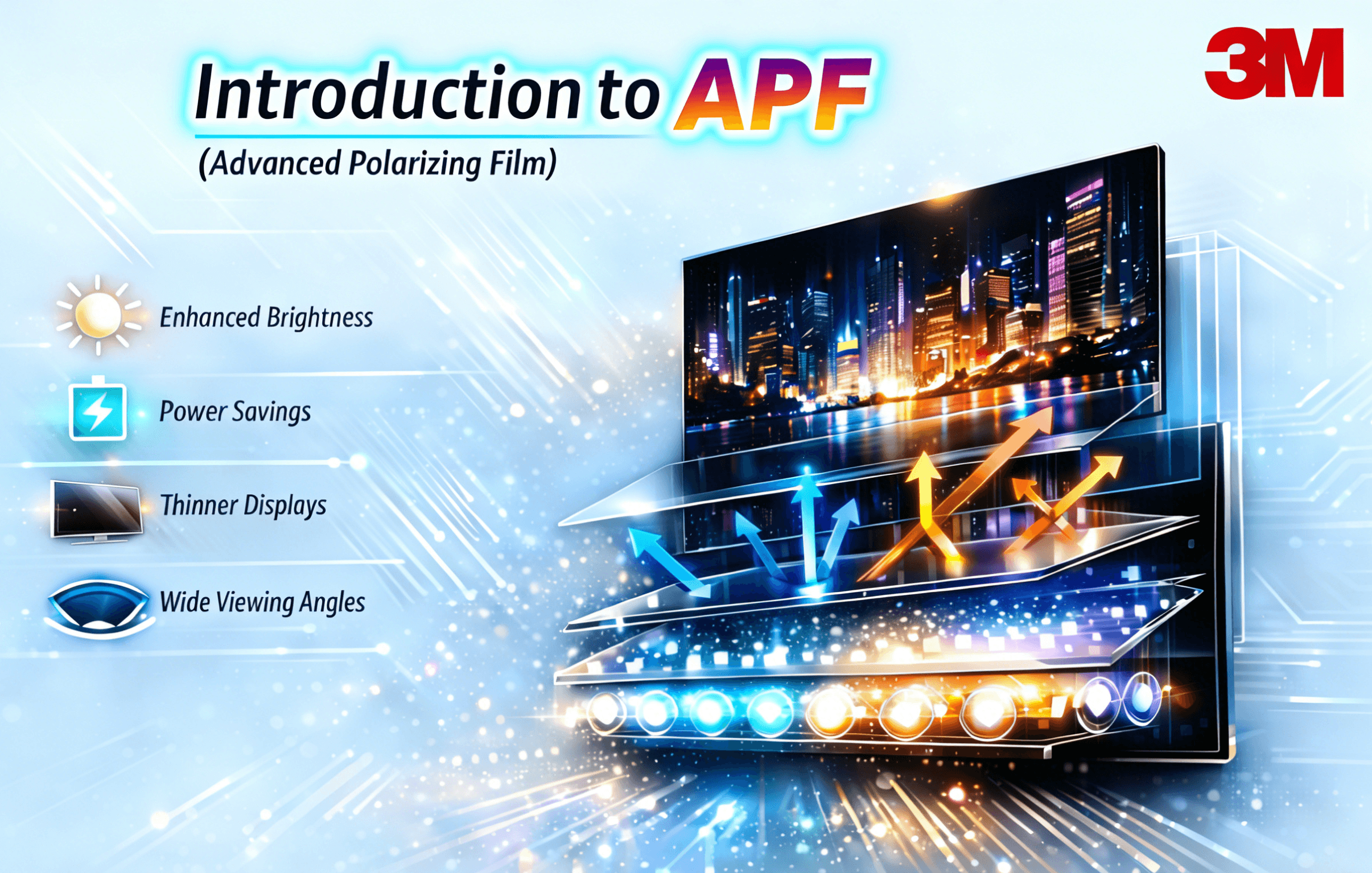
Introduction to APF (Advanced Polarizing Film)
3M’s APF (Advanced Polarizing Film) is not a traditional “absorptive polarizer.” Instead, it is an on‑glass reflective polarizer applied directly to the LCD glass. Its primary functions are to improve backlight efficiency, increase brightness, reduce module thickness, and enhance display performance from wide viewing angles.
As shown in the picture below, APF allows the polarization direction required by the LCD to pass through, while reflecting the orthogonal polarization back into the backlight system. The reflected light undergoes multiple scatterings inside the backlight cavity, and part of it returns with a rotated polarization state that can be reused. In other words, APF recycles light that would otherwise be wasted, thereby improving brightness and energy efficiency.

Reference: https://www.3m.com/3M/en_US/p/d/b5005047084/
Advantages of APF
-
Brightness Enhancement (by around 30%)
Reduces optical loss and improves both on‑axis and wide‑angle brightness.
-
Power Savings
By increasing backlight efficiency, APF reduces backlight power consumption, helping achieve lower energy usage and longer battery life.
-
Thinner Module
Since APF is laminated directly on glass, it can replace part of the BEF/DBEF stack, simplifying the optical structure.
-
Better Viewing‑Angle Performance
The reflective polarizer structure improves brightness uniformity and wide‑angle brightness.
-
Higher Environmental Robustness
More stable than “free‑standing reflective films,” with lower thermal load and better durability.
Comparison Between APF and DBEF
| Item | APF (Advanced Polarizing Film) | DBEF (Dual Brightness Enhancement Film) |
| Basic Type | On‑glass reflective polarizer (laminated on LCD glass) | Backlight reflective polarizer (placed inside the backlight module) |
| Installation Position | Laminated directly on the rear polarizer of the LCD (on‑panel laminate) | Located inside the backlight system (typically above the light guide plate) |
| Primary Function | Transmits the required polarization and reflects the orthogonal polarization back to the backlight cavity to improve polarization efficiency | Recycles absorbed polarization to increase backlight brightness |
| Brightness Gain | ~30% (per 3M), with better wide‑angle brightness retention | Typically 30–60%, but more viewing‑angle dependent |
| Energy Efficiency | Higher efficiency → lower backlight power → longer battery life | Higher brightness → potential for lower backlight power |
| Thickness Impact | Thinner; reduces BEF/DBEF stacking; ideal for narrow‑bezel designs | Thicker; adds layers to the backlight stack |
| Viewing‑Angle Performance | Superior wide‑angle brightness | Strong viewing‑angle dependence; off‑axis brightness drops significantly |
| Integration Level | High (on‑glass integration) | Medium (backlight component) |
| Environmental Robustness | Higher (on‑glass structure is more stable with lower thermal load) | More affected by backlight cavity temperature |
| Indentation Resistance | Hard‑coat surface reduces pressure marks | No hard‑coat; more susceptible to mechanical pressure |
| Typical Applications | Smartphones, tablets, laptops, VR, IoT devices | Smartphones, tablets, laptops, large‑size displays |
| Typical Models | APF‑QWP, APF‑V3‑26, APF‑T35 | DBEF6, DBEF‑D, DBEF‑E, etc. |
| Cost | Higher (due to high integration and on‑glass lamination) | Medium (standard backlight material) |
| Design Targets | Thin‑and‑light designs, narrow bezels, high efficiency, wide viewing angles | High brightness, cost‑sensitive designs, traditional backlight structures |
Based on the comparison above, we will recommend APF when you need thinness, efficiency, and wide‑angle performance, and DBEF when you need maximum brightness at lower cost.
Should you have any questions, please consult our engineering.
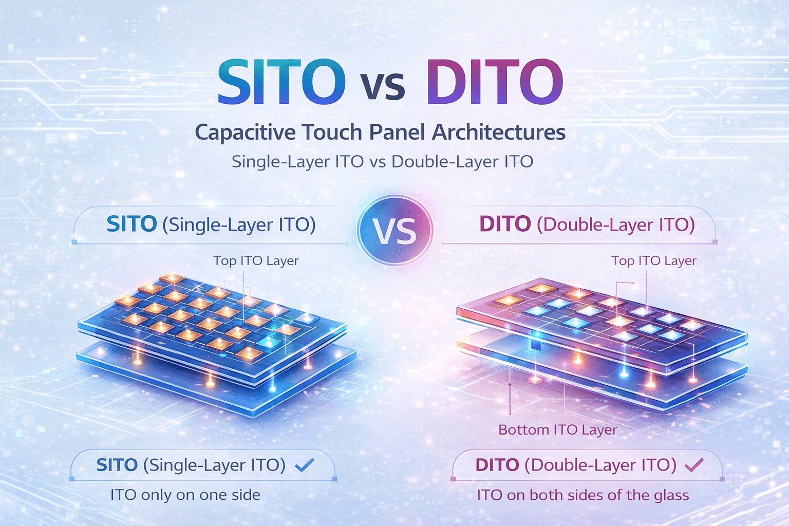
SITO vs DITO Touch Panel Architecture
Capacitive Touch detects touch by measuring changes in capacitance across a matrix of electrodes. Thus the core design question is: How do we arrange X and Y electrodes?
The two mainstream architectures in industry now are SITO (Single-layer ITO) and DITO (Double-layer ITO).
The core difference lies in whether the ITO is formed on both sides of the glass (DITO) or only on one side (SITO).

The red shadow in the image above indicates the ITO layer
DITO is patented by Apple and offers lower cost. For international customers, it is generally necessary to avoid using DITO.
SITO does not mean there is only a single ITO layer. It can also have multiple ITO layers. For example, in the case below, it is a SITO structure but includes two ITO layers (and it can have even more). The transmitter (Tx) and receiver (Rx) electrodes can be implemented on the same layer or on different layers, and there can also be additional jump/bridge layers.
Below is the 3D image show the SITO structure:

For a SITO design, both X and Y electrodes are implemented on a single ITO layer
SITO integrates both Tx and Rx electrodes on the same surface, which requires careful pattern design and layer management to ensure proper electrical isolation while maintaining stable capacitive coupling. In practice, SITO does not imply a single ITO layer; multiple conductive layers can be implemented on the same side by introducing insulating layers in between, allowing Tx and Rx to be arranged either on the same layer or on different stacked layers.
To achieve routing without electrical interference, additional structures such as bridges or jumpers are often used, enabling signal lines to cross over one another within a compact layout.
See below:

On the left, each diamond-shaped electrode represents an individual sensing unit, with the Tx and Rx electrodes arranged in an interleaved pattern through these diamond structures. Since all electrodes are located on the same side, direct routing would inevitably lead to signal lines blocking or intersecting each other. This is where the crossover structure becomes necessary. The positions labeled “crossovers” in the diagram are typical bridge points.
A bridge (or jumper) essentially works by locally elevating one signal line to cross over another. In practice, this is achieved by first forming a routing line on the bottom ITO layer, then covering it with a dielectric (insulating) layer, and subsequently adding a short conductive bridge on top (which can be made of ITO or metal). This allows the signal to “pass over” the other line before returning to the original layer. By separating the lines vertically in this way, electrical shorting is avoided.
Compared with DITO, SITO offers greater flexibility in avoiding patent constraints and is more suitable for global markets; however, it comes with increased process complexity, placing higher demands on alignment accuracy, dielectric uniformity, and yield control of bridge structures, while also requiring careful optimization between optical performance and electrical characteristics.
On the right, DITO can be understood as a structure in which the Tx and Rx electrodes are physically separated onto two different sides of the substrate, typically on opposite surfaces of the glass. In the “Two Layers Design” illustration, this separation is conceptually similar: the electrodes are distributed across different layers, so routing conflicts are inherently avoided.
Unlike SITO, where all electrodes share the same side and require bridge or jumper structures to cross over one another, DITO achieves this separation naturally by placing one set of electrodes (for example, Tx) on the top surface and the other set (Rx) on the bottom surface. As a result, there is no need for local crossover structures, since the signal lines do not compete for space within the same plane.
This architecture simplifies the pattern design and reduces process complexity related to bridge formation, dielectric deposition, and alignment of multi-layer routing on a single side. It also improves electrical performance consistency, since there are fewer discontinuities such as bridge transitions. However, DITO requires double-sided processing, including alignment between the two surfaces of the glass, which introduces its own manufacturing challenges.
If you have any questions, please contact our engineering.
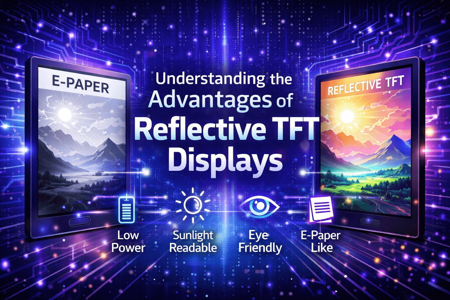
Introduction of Reflective TFT
When it comes to low-power display technologies, reflective TFT displays are becoming an increasingly popular choice. In fact, many customers who see them for the first time often compare them to e-paper—and for good reason.
Both technologies share several attractive benefits: low power consumption, excellent sunlight readability, eye comfort, and a paper-like viewing experience. But despite these similarities, reflective TFT offers some important advantages that set it apart.
Reflective TFT vs. E-Paper: What’s the Difference?
Wider Operating Temperature Range
Most e-paper displays are designed to operate within a temperature range of 0°C to 50°C. Reflective TFT, on the other hand, can typically function in a much wider range—from -20°C to 80°C.
This makes reflective TFT a better option for outdoor or industrial environments where temperature conditions can vary significantly.
Faster Refresh Rate
One of the key limitations of e-paper is its slow refresh speed. While it works well for static content, it struggles with dynamic tasks like:
- Scrolling webpages
- Opening new tabs
- Displaying animations
Reflective TFT displays don’t have this limitation. Their faster response time makes them much more suitable for applications that require smooth, real-time interaction.
Better Color Performance
E-paper displays are typically limited in color capability:
- Most are black and white
- Some support up to 3 colors
Reflective TFT displays offer far more flexibility:
- Black & white
- 4 or 8 colors
- Full color (up to 16.7 million colors)
This makes reflective TFT a strong candidate for applications where visual richness matters.
Compared to Traditional TFT (IPS/TN)
Unlike standard IPS or TN TFT displays, reflective TFT does not require a backlight under normal conditions. This brings several benefits:
- Thinner display structure
- Lower power consumption
- Excellent visibility in bright sunlight
While IPS displays may require high brightness levels (e.g., 1000 nits) to remain readable outdoors, reflective TFT uses ambient light instead—making it naturally sunlight-readable.
At the same time, it remains eye-friendly for indoor use, providing a comfortable viewing experience similar to paper.


Power Consumption: What to Expect
The power consumption of reflective TFT varies depending on screen size and color depth. Here are some typical examples:
- Black & White (1.54”–4.2”)
~0.08 to 0.10 mW - 4 / 8 Color Displays
~0.10 mW (2”) up to ~40 mW (8”) - Full Color (16.7M colors, ~5”)
~350 mW
At higher brightness levels (e.g., when using a backlight at ~35 nits), power consumption can approach that of IPS TFT (~1000 mW). However, a key advantage is that reflective TFT does not require the backlight to be constantly on, helping reduce overall energy usage in real-world applications.

Final Thoughts
Reflective TFT displays bridge the gap between traditional TFT and e-paper technologies. They combine:
- The low power and readability of e-paper
- The speed and color performance of TFT
This unique balance makes them an excellent choice for a wide range of applications—from portable devices to outdoor equipment.
If you’re looking for a display that delivers both performance and efficiency, reflective TFT is definitely worth considering.
If you have any questions, please contact our engineering.
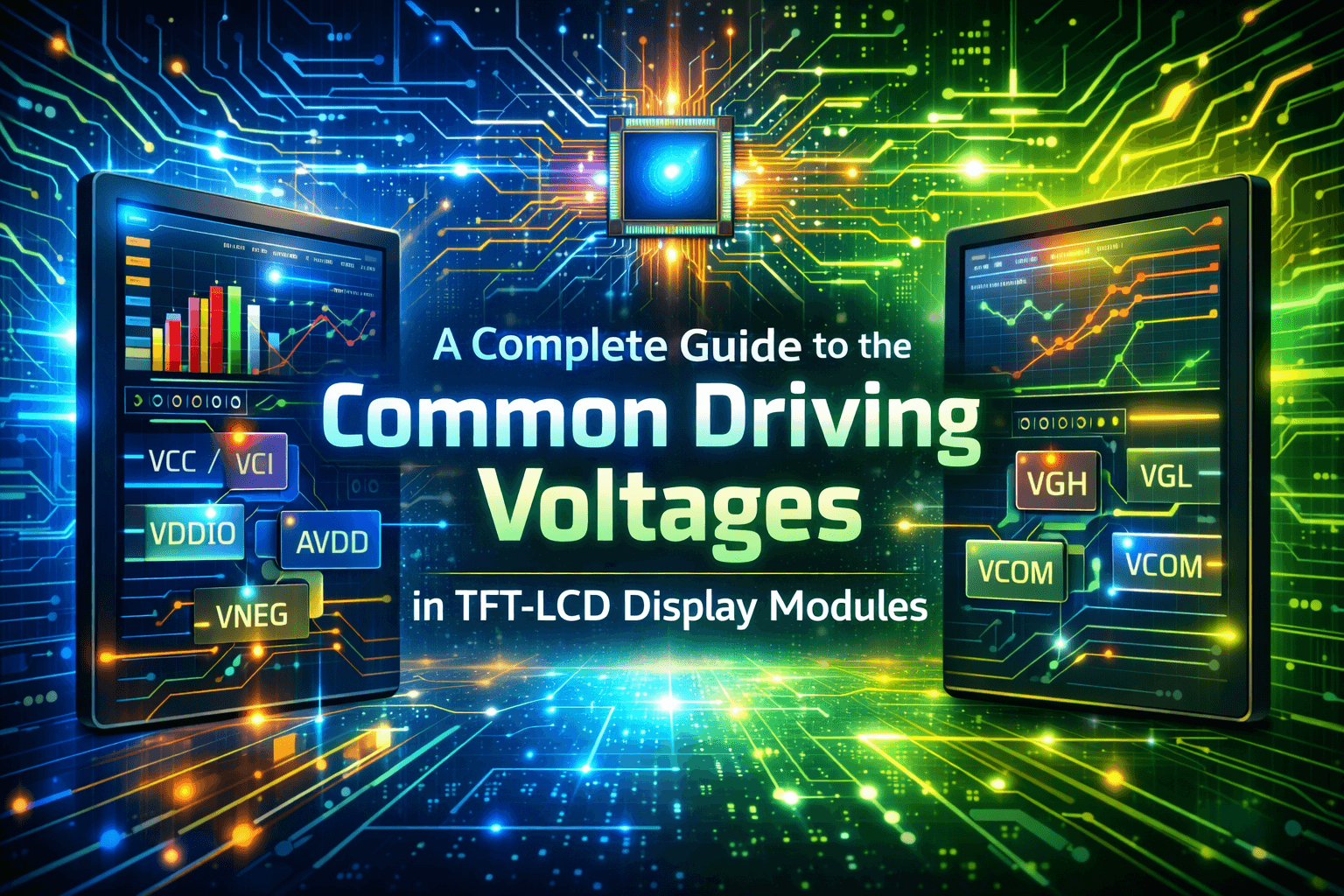
A Complete Guide to the Functions of Common Driving Voltages in TFT-LCD Display Modules
We will explain several common driving voltages in a TFT-LCD module from an engineer’s perspective: what each voltage rail does, the typical voltage ranges, which components use them, and what needs attention during design.
What voltage rails are present in a TFT-LCD module
Typical small- to medium-size TFT-LCD modules commonly include the following voltage rails:
- VCC / VCI: Digital core power supply (MCU/interface logic)
- VDDIO: I/O power supply (pixel data/control signal interfaces)
- AVDD (or the positive rail in VPOS/VNEG): Analog power supply for the source driver IC and the upper limit of the pixel voltage range
- VNEG (sometimes called VNS, VGLS, etc.): Negative power supply for the source driver and the lower limit of the pixel voltage range
- VGH: Gate high voltage, the TFT gate “ON” voltage
- VGL (or VEE, GVEE, etc.): Gate low voltage, the TFT gate “OFF” voltage, typically a negative voltage
- VCOM: Common electrode reference voltage (Common Electrode), which determines the center point of the liquid crystal’s alternating drive
Many dedicated PMICs (such as TPS65156, for example) are designed specifically to convert a single 3.3–5 V input into the multiple voltage rails above for TFT-LCD panels and their driver ICs.
VCC / VCI / VDDIO: Digital Logic and Interface Power
Function
- Supplies power to the internal digital circuits of the LCD driver IC, timing logic, and interface controller (such as RGB/8080/SPI interface logic).
- Powers the I/O buffers connected to the main controller SoC (e.g., VDDIO), ensuring voltage-level compatibility such as 3.3 V or 1.8 V.
Typical Range
- VCC / VCI: Generally 2.5–3.3 V; some driver ICs support down to 1.8 V.
- VDDIO: Common values are 1.8 V / 2.8 V / 3.3 V, matching the I/O voltage of the host controller.
Engineering Considerations
- Power-up sequence: Digital power and logic levels usually need to stabilize before or at the same time as analog voltages such as AVDD and VGH/VGL, to prevent the driver IC from entering an abnormal state (see the specific IC datasheet for details).
- Signal level matching: The I/O voltage of the main controller must match the module’s VDDIO; otherwise, level shifting is required.
AVDD / VPOS / VNEG: Source Driver Analog Power and Pixel Voltage Range
Function
- AVDD (or the VPOS/VNEG pair) is the power supply rail for the analog output of the source driver, used to store a voltage corresponding to each pixel’s grayscale level.
- The source driver outputs different voltage levels between AVDD and VNEG to each subpixel capacitor, thereby changing the voltage difference across the liquid crystal and adjusting light transmission.
Typical Range
- AVDD: Typically between 8–15 V, commonly 9–13 V, with current in the tens of milliamps range; it is one of the main sources of power consumption.
- VNEG: Often the negative counterpart of AVDD, such as around ±7 V, giving an overall pixel voltage range of approximately +7 V to −7 V.
Engineering Considerations
- Load current: AVDD supplies the entire source driver output stage, so sufficient current capability and low ripple are required. Otherwise, grayscale levels may fluctuate with image changes, causing effects such as “breathing” or flickering.
- Voltage range: This directly determines the available pixel voltage swing, which in turn affects contrast and the adjustable range of the gamma curve.
- Generation method: Commonly produced using a boost DC-DC converter plus a charge pump, with output set via feedback resistors (for example, in some designs AVDD is determined by the resistor divider of a boost chip such as RT9293).
VGH / VGL: TFT Gate Switching Voltages (Gate Driver)
Function
- The Gate Driver provides high/low levels to the gate of each row of TFTs to implement row scanning:
- VGH: Gate “ON” voltage. The TFT turns on, connecting the pixel capacitor of the current row to the source data line.
- VGL: Gate “OFF” voltage, usually negative, ensuring the TFT is fully turned off and the pixel voltage is held until the next frame refresh.
Typical Range
- VGH: Generally around +12 to +25 V, with relatively small current demand, typically a few mA to about 10 mA.
- VGL (or VEE, GVEE): Usually −5 V to −15 V, typically −6 to −10 V, also with low current demand.
Why Such “High” and “Negative” Voltages Are Needed
- The TFT threshold voltage is limited. If only 0–3.3 V were used, it would be difficult to achieve both strong conduction when on and complete cutoff when off, resulting in leakage and severe image retention.
- Using a VGH much higher than the maximum source/pixel voltage ensures strong conduction, while using a VGL lower than (or even more negative than) the most negative source/pixel voltage ensures reliable cutoff, reducing leakage and crosstalk.
Engineering Considerations
- Stability: Transients and noise on VGH/VGL can directly appear as flicker or row noise, so proper decoupling and controlled rise/fall edges are required.
- Generation method: Often generated from AVDD using a charge pump or voltage-doubling/inverting circuits, such as simple topologies where VGH ≈ 2 × AVDD and VGL ≈ −AVDD.
VGH / VGL: TFT Gate Switching Voltages (Gate Driver)
Function
- The Gate Driver provides high/low levels to the gate of each row of TFTs to implement row scanning:
- VGH: Gate “ON” voltage. The TFT turns on, connecting the pixel capacitor of the current row to the source data line.
- VGL: Gate “OFF” voltage, usually negative, ensuring the TFT is fully turned off and the pixel voltage is held until the next frame refresh.
Typical Range
- VGH: Generally around +12 to +25 V, with relatively small current demand, typically a few mA to about 10 mA.
- VGL (or VEE, GVEE): Usually −5 V to −15 V, typically −6 to −10 V, also with low current demand.
Why Such “High” and “Negative” Voltages Are Needed
- The TFT threshold voltage is limited. If only 0–3.3 V were used, it would be difficult to achieve both strong conduction when on and complete cutoff when off, resulting in leakage and severe image retention.
- Using a VGH much higher than the maximum source/pixel voltage ensures strong conduction, while using a VGL lower than (or even more negative than) the most negative source/pixel voltage ensures reliable cutoff, reducing leakage and crosstalk.
Engineering Considerations
- Stability: Transients and noise on VGH/VGL can directly appear as flicker or row noise, so proper decoupling and controlled rise/fall edges are required.
- Generation method: Often generated from AVDD using a charge pump or voltage-doubling/inverting circuits, such as simple topologies where VGH ≈ 2 × AVDD and VGL ≈ −AVDD.
Relating the Voltage Rails to Display Performance
We can connect these voltages from the perspective of an equivalent circuit of a single pixel:
- Row selection: When a row is driven to VGH by the Gate Driver, all TFTs in that row turn on. The source driver then writes the corresponding data voltage into the pixel capacitor (relative to VCOM).
- Row off: The gate voltage returns to VGL, turning the TFT off. The pixel capacitor holds the voltage that was just written until the next refresh.
- Grayscale control: The source output voltage varies within the AVDD/VNEG range, creating different amplitudes and polarities of voltage between the pixel electrode and VCOM, which changes light transmission and produces levels from black to white and intermediate grayscale.
- Alternating drive: The polarity is inverted between frames or rows so that the average voltage across the liquid crystal remains close to zero. The human eye perceives only the change in transmittance, which prevents DC damage to the liquid crystal.
A Concise Engineering Intuition:
- VCC / VDDIO determine whether the system can receive commands and data.
- AVDD / VNEG determine how bright or dark a pixel can be driven.
- VGH / VGL determine whether a row of pixels can be reliably written and held.
VCOM determines the center voltage for positive/negative alternation and influences overall contrast and flicker behavior.
If you have any questions, please contact our engineering.
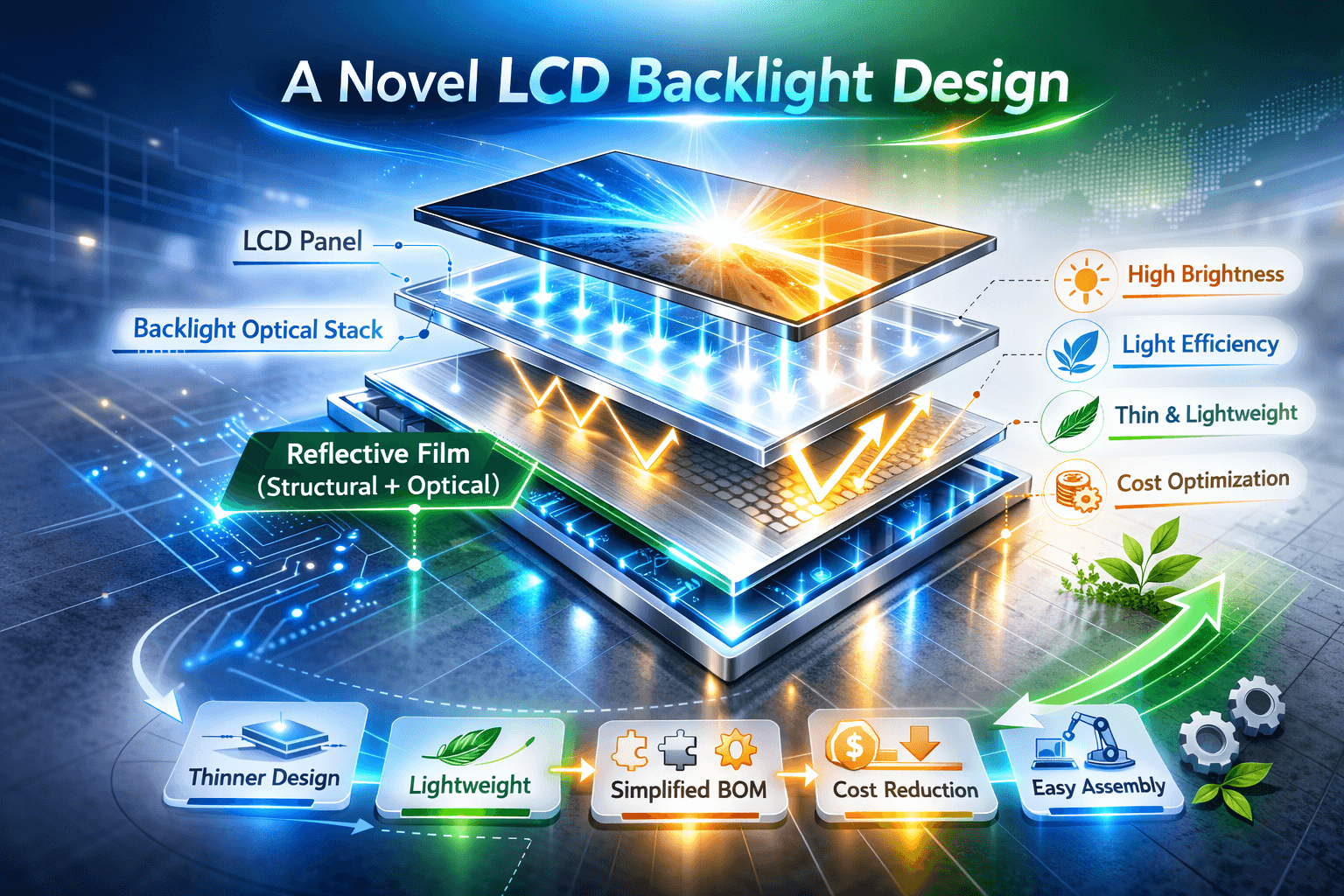
A Novel LCD Backlight Design
A reflective film is an optical component used within a display’s backlight assembly to recycle light and increase brightness/efficiency, whereas a plastic backlight is a type of complete backlighting unit structure, often utilizing an edge-lit design with light guide plates and various films, including a reflective film as its bottom layer.
The Optical Reflective Film for Liquid Crystal Display (LCD) market refers to a specialized segment in the electronics and display technology industries, driven by the growing demand for high-quality visual experiences. Optical reflective films are primarily used in LCD panels to improve their brightness and contrast by reflecting and optimizing light. These films contribute to enhancing the clarity, color accuracy, and overall display performance of devices like televisions, smartphones, tablets, and monitors. The global demand for such technology has surged in recent years, as consumers and businesses alike seek displays with superior image quality and energy efficiency.

Traditional Module Structure
- LCD Glass
- Backlight Optical Stack
- Backlight Reflector Sheet
- Plastic Frame / Plastic Housing
- Metal Back Plate
Functional separation
- Optical function: Backlight reflector
- Structural function: Plastic frame
- Encapsulation function: Frame + back shell
Reflective Film Bottom Design (Intergraded Structure)
- LCD Glass
- Backlight Optical Stack
- Reflective Film (Structural + Optical)
- Integrated Sealing Layer (No Plastic Frame)
Integrated Functionality
- Optical Reflection
- Bottom Packaging
- Structural Support
- Module Fixing
- Thickness Control
In order to achieve below Engineering Objectives
- Module thinning design
- Lightweight structure
- Simplified BOM structure
- Optimized cost structure
- Automation-friendly assembly
- Integrated module design
Overall, compared with a conventional plastic backlight housing, the reflective-film bottom design achieves a thinner profile and lower weight, while the plastic backlight structure provides higher mechanical robustness.

Q&A for Reflective Film Bottom design
Question 1: Are the Reflective film bottom design meets structural strength and aging resistance requirements?
Answer: It meets the requirements. The structural strength must not only be provided by the LCD module itself, but the overall structure of the complete device housing must also protect the LCD module. In terms of aging test, it is no different from products with plastic frame bottom sealing.
Question 2: Is it able to meet the compatibility of thermal expansion and contraction?
Answer: Yes, Orient Display factory able to meet this requirement.
Question 3: Is the Reliability testing (vibration, drop, thermal cycling), will also be performed for reflective film bottom design LCD?
Answer: Yes, Orient factory able to perform the same Reliability test accordingly.
Question 4: Is the reflectivity able meet the backlight luminous efficacy requirements?
Answer: Yes, we can meet this requirement.
Question 5: Is the bottom sealing structure able to meet IP protection design requirements?
Answer: There is no problem with dust protection. However, the waterproof performance of an individual product is slightly worse than that of a product with a sealed bottom frame. If the entire machine is properly protected, the performance is the same.
If you have any questions, please contact our engineering.
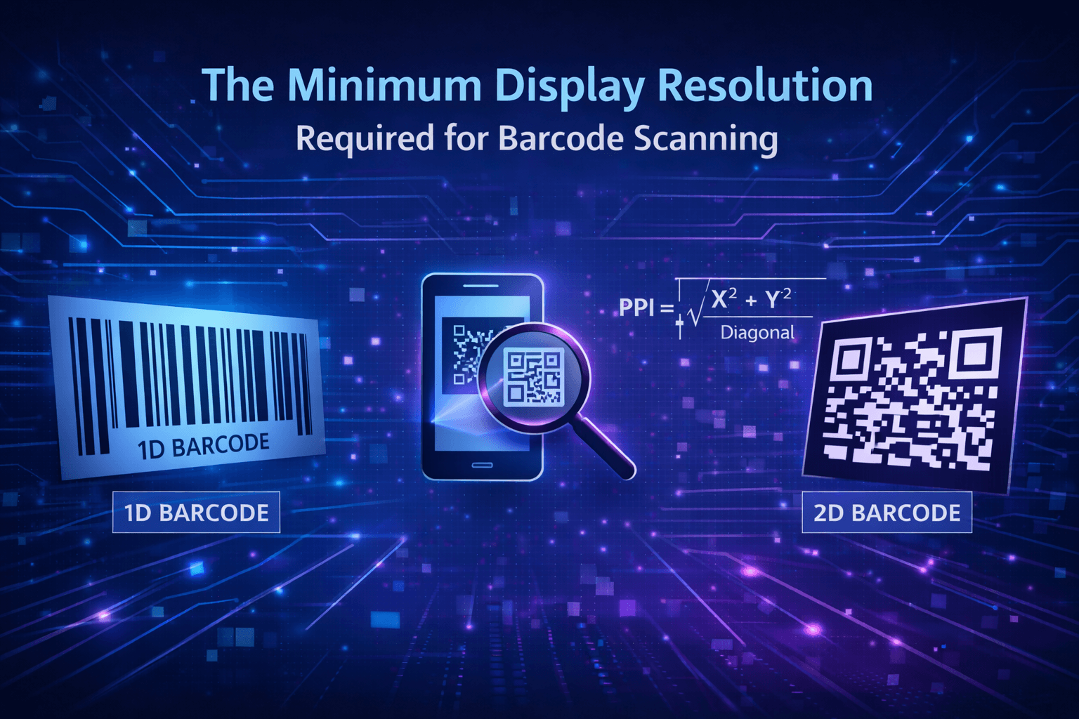
The Minimum Display Resolution Required for Barcode Scanning
Types of Barcodes
The types of barcodes can be divided into two main categories:

1. One-Dimensional Barcodes (1D Barcode)
Features:
Encodes data only in the horizontal direction, suitable for short sequences of numbers or letters. Commonly used in retail, logistics, and industrial systems.
| Barcode Type | Features | Common Uses |
| EAN-13 / EAN-8 | Numeric only (0–9), includes a check digit; international standard for retail barcodes | Supermarkets, retail products |
| UPC-A / UPC-E | North American standard, similar to EAN | Retail packaging |
| Code 39 | Supports letters, numbers, and some symbols; variable bar width | Industry, warehousing, military |
| Code 128 | High density, supports full ASCII; encodes long strings | Logistics, healthcare, tickets |
| Interleaved 2 of 5 (ITF-25) | Numeric only; interleaved structure | Carton codes, shipping packages |
| Codabar | Numbers + specific start/stop characters (A–D) | Libraries, blood banks, legacy systems |
| MSI / Plessey | Numeric, older format | Internal retail systems |
Common selection recommendations:
- For retail products → use EAN-13 / UPC-A
- For internal codes, warehousing, or custom text → use Code 128 (most versatile)
2. Two-Dimensional Barcodes (2D Barcode)
Features:
Encodes information in both horizontal and vertical directions, allowing much more data storage. Most can be scanned by smartphones.
| Barcode Type | Features | Common Uses |
| QR Code | Most widely used; supports numbers, letters, Chinese characters, and binary; built-in error correction | Payments, URLs, product traceability |
| Data Matrix | Compact size, high error correction, easily recognized by industrial cameras | Chips, electronic components, medical devices |
| PDF417 | Stacked linear format, can encode long text | Boarding passes, ID cards, logistics labels |
| Aztec Code | No need for an external quiet zone, suitable for small areas | Tickets, mobile interfaces |
| MaxiCode | Developed by UPS for logistics | International parcel sorting systems |
Common selection recommendations:
- For smartphone scanning → QR Code
- For factory, metal, or small component marking → Data Matrix
3. How to Choose
| Application | Recommended Barcode Type |
| Retail sales (recognized by POS systems) | EAN-13 / UPC-A |
| Internal asset or workstation labeling | Code 128 |
| Mobile scanning (URLs, info display) | QR Code |
| High-density, small-size, industrial scanning | Data Matrix |
| Very limited printing space but still scannable | Aztec |
Barcode Display Resolution Requirements
1. Concept of PPI
PPI (Pixels Per Inch) refers to the number of pixels contained in one inch (25.4 mm) of display length.
It indicates the pixel density or level of detail of the screen — the higher the PPI, the denser the pixels, and the smoother and sharper the images and text will appear.
Formula:

Alternatively, for one direction (horizontal or vertical):

Example: Orient Display E-Paper AES200200A00-1.54ENRS
- Active Area (AA): 27 mm × 27 mm (≈ 1.063 in × 1.063 in)
- Resolution: 200 × 200 pixels
- Pixel Pitch: 0.135 × 0.135 mm

Or equivalently, using pixel pitch:

Quick Reference Table
| Pixel Pitch | Equivalent PPI |
| 10 mil (0.254 mm) | 100 ppi |
| 7.5 mil (0.191 mm) | 133 ppi |
| 6.5 mil (0.165 mm) | 154 ppi |
| 5 mil (0.127 mm) | 200 ppi |
| 2.5 mil (0.064 mm) | 400 ppi |
2. Resolution Requirements for Common 1D Barcodes
a. EAN-13 / EAN-8 / UPC-A / UPC-E (Retail Codes)
- Typical X dimension: 0.33 mm (13 mil)
- Recommendation: Minimum 2 pixels per narrow bar
- Required PPI:

- Practical Recommendation:
≥ 150 ppi usable, ≥ 200 ppi preferred- At 27 mm active area:
- 150 ppi → ~160×160 px
- 200 ppi → ~213×213 px
- At 27 mm active area:
b. Code 128 (Logistics / Internal Encoding, Very Common)
- Typical X dimension: 0.25 mm (10 mil)
- Required PPI:

- Recommendation:
≥ 200 ppi preferred, especially for longer codes.
At ~150 ppi, the barcode must be enlarged and simplified to avoid crowding.
c. Code 39, ITF-25, Codabar, MSI, etc.
- Lower density, mostly for internal management.
- Typical X dimension: 0.33–0.5 mm
- Recommended PPI: ≥ 120–150 ppi
- Practical Note:
150 ppi is generally sufficient; less demanding than Code 128.
3. Resolution Requirements for 2D Barcodes
2D barcodes rely on module size (the smallest square unit). Each module should ideally be represented by at least 2 pixels.
a. QR Code
- Typical module width: 0.3–0.5 mm
For 0.3 mm modules:

- Recommendation:
Minimum ~170 ppi, recommended ≥ 200 ppi- On a 27 mm, 200 ppi display → ~213×213 px — sufficient for medium-size QR codes.
b. Data Matrix
- Used for small components and chips; modules can be very small (0.2–0.3 mm).
- For 0.2 mm modules:

- Recommendation:
≥ 250 ppi suitable, 300 ppi preferred for industrial use.
If the screen is only 200 ppi, enlarge the Data Matrix (module ≥ 0.25–0.3 mm).
c. PDF417 / Aztec Code
- High-density symbologies; require higher pixel density.
- PDF417: ≥ 200–250 ppi recommended
- Aztec: ≥ 200 ppi minimum; 300 ppi preferred when space is limited
4. Summary for 27 mm × 27 mm E-Paper Displays
| Barcode Type | Minimum Usable PPI | Recommended PPI | Recommended Pixels (27 mm area) |
| EAN / UPC | ≥150 ppi | 200 ppi | ≈ 213×213 |
| Code 39 / ITF-25 | ≥150 ppi | 200 ppi | ≈ 213×213 |
| Code 128 | ≥200 ppi | 250–300 ppi | 213×213 / 320×320 |
| QR Code | ≥170 ppi | 200–300 ppi | 213×213 / 320×320 |
| Data Matrix | ≥250 ppi | 300 ppi | ≈ 320×320 |
| PDF417 / Aztec | ≥200 ppi | 250–300 ppi | ≥ 213×213 |
If you have any questions, please contact our engineering.
Working Principles and Structure of TFT LCD Backlight
What is a backlight
LCDs themselves do not emit light, so they require an external planar light source system to enable image display. This system is called a backlight (Backlight).

Types of backlights
Based on the light emission method, backlights can be divided into direct-lit (direct-type) and edge-lit (side-lit) types. Among them, edge-lit backlights are widely used in small- and medium-sized applications, such as mobile phones, tablets, and computers.

Working principle
The working principle of a backlight is to convert a point light source into a uniform surface (area) light source, providing the external illumination required for LCD display.

Composition of an edge-lit backlight
An edge-lit backlight mainly consists of a light bar (LED + FPC), light guide plate (LGP), reflector sheet (R), diffuser film (D), and brightness enhancement film (prism film, BEF), among other components.

1. LED (Light Emitting Diode)
An LED is the light source of the backlight module. Together with the FPC, it forms what is commonly referred to as the light bar (Light Bar).
The light-emission principle of an LED is as follows:

An LED emits light through electroluminescence. When a forward voltage is applied, electrons and holes recombine in the PN junction, releasing energy in the form of photons, thereby producing visible light.
2. Light Guide Plate (LGP)
A linear light source array composed of LEDs injects light into the light guide plate from one side. The light propagates inside the LGP and strikes the micro-dot patterns on the plate, where scattering occurs. As a result, the light exits from the surface of the LGP without dot patterns, forming a uniform surface light source.

3. Reflector
The reflector reflects the light that leaks from the bottom of the LGP back into the light guide plate for reuse, thereby increasing light utilization efficiency.

4. Diffuser
The diffuser uniformizes the light passing through it by refraction and scattering caused by acrylic beads, rough surfaces, or diffusing particles within the film. This process effectively evens out the light distribution and helps mask luminance non-uniformities and defects.

5. Brightness Enhancement Film (BEF)
BEF, also known as a prism film, has a light-concentrating function that increases display brightness. As shown below, among the three commonly used film-stack configurations, the high-brightness solution is clearly 2 BEF + 1 DBEF. BEF works by using micro-prism structures to redirect scattered light into the viewing direction, thereby improving on-axis luminance. DBEF (Dual Brightness Enhancement Film) further enhances efficiency by recycling polarized light, resulting in a noticeable brightness gain when combined with BEF.

6. Dimming methods
There are two mainstream backlight dimming methods: DC dimming and PWM dimming. In addition to these, MIX dimming is also a commonly used dimming mode today.
If you have any questions, please contact our engineering.
For more information about backlight, please visit our Knowledge Base.
Methods for Securing TFT and OLED Display Panels in an Enclosure
Most Common Mounting Methods (Consumer Displays / Laptops)
1. Front Bezel Snap-Fit
Principle
- The panel is inserted from the front
- A plastic front bezel uses snap-fit clips to hold the panel around its perimeter
- The rear cover is then assembled as a whole
Pros
- Low cost and fast assembly
- No screws required (or very few)
Cons
- Moderate impact resistance
- Snap clips are prone to damage after repeated disassembly
Commonly Used In
- Laptop computers
- Low-cost monitors
- All-in-one PC front housings
2. Screw + Bracket Mounting (Most Secure)

Principle
- The four corners and/or edges of the panel have VESA or M2/M3 mounting holes
- The panel is fastened to the rear housing using PCB, metal, or plastic brackets
- The front bezel is used only for decoration and dust protection
Pros
- High structural strength
- Controlled load on the panel (prevents glass damage)
- Easy to service and repair
Cons
- Slightly higher cost
- More assembly steps
Commonly Used In
- Desktop monitors
- Industrial displays
- Medical / commercial equipment
Thin and Bezel-Less Display Solutions

3. Double-Sided Tape / OCA Adhesive Bonding
Principle
- High-strength double-sided tape (such as 3M VHB) or high-strength adhesives are applied along the panel edges
- The panel is bonded directly to the mid-frame or metal backplate
Pros
- Ultra-thin and minimalist design
- Excellent appearance (narrow bezels)
Cons
- Difficult to repair or rework
- High requirements for assembly precision
- Thermal expansion and contraction must be carefully considered
Commonly Used In
- Ultra-thin displays
- OLED displays
- Tablets / high-end all-in-one PCs
4. Metal Mid-Frame Clamping (High-End Approach)
Principle
- The panel is placed into a CNC-machined metal mid-frame
- Slight clamping lips are formed around the perimeter
- Screws secure the backplate, creating an overall clamping structure
Pros
- Extremely high rigidity
- Even stress distribution on the panel
- Good thermal dissipation
Cons
- High cost
- Complex mechanical design
Commonly Used In
- High-end professional monitors
- Industrial control displays
- High-brightness outdoor displays
Industrial / Automotive / Vibration-Resistant Applications

5. Backplate Tray + Shock-Absorbing Pads
Principle
- The panel is placed on a metal tray
- Silicone or foam shock-absorbing pads are added around the perimeter
- Screws are used to secure the assembly without directly pressing on the panel
Characteristics
- Excellent vibration and impact resistance
- Prevents stress concentration on the glass
- Long service life
Cons
- Thicker overall structure
Commonly Used In
- Automotive displays
- Military / industrial equipment
- Outdoor devices
A Typical “Combined Structure” of a Display
- Front Bezel (snap-fit / decorative)
- Panel (LCD / OLED)
- Foam / Double-Sided Tape / Brackets
- Metal Mid-Frame / Plastic Frame
- Main PCB + Backplate
In real products, multiple methods are almost always combined, for example:
- Snap-fit + screws
- Adhesive bonding + mid-frame
- Tray + shock-absorbing pads + screws
Common Design Pitfalls (Very Important)
1. Never press directly on the glass with screws
- Brackets or pressure plates must be used
2. Leave clearance at the edges for thermal expansion
- LCD panels can deform under temperature changes
3. Avoid localized stress
- Otherwise, “Newton rings / mura / dark spots” may appear
4. Provide strain relief for flex cables
- FPCs must have sufficient bend radius
If you have any questions, please contact our engineering.
A High Transparent LCD Display
A High Transparent LCD Display without using polarizer has been development. Its name is Polymer Nematic Liquid Crystal Display (PNLC). A PNLC is a nematic liquid crystal system lightly cross-linked with a polymer network formed by in-situ photopolymerization so that the Liquid Crystal will present off and on states in the electrified state. This puts PNLC between: Conventional nematic LCDs (TN / IPS / VA) and Polymer-dispersed systems (PDLC).

How PNLC Works (Step-by-Step)
-
Material Structure
- Nematic LC host (high birefringence is common)
- ~1–5 wt% polymerizable monomer
- UV curing forms a continuous but sparse polymer network
-
Optical States
OFF state (no field):
- LC director is distorted by polymer anchoring
- Produces:
- Controlled scattering, or
- Randomized birefringence
ON state (electric field applied):
- LC aligns with the field
- Polymer network limits flow but allows reorientation
- Optical state becomes uniform


Key Features
- Transparent with transmission rate: ~90% (without polarizer used)
- Fast response: ~20ms at 10V, ~120ms at 5V
- Contrast Rate (CR): ~3.
- Vop: 3.3-10V
- Current consumption: 1mA/3.3V
- Interface: Parallel, SPI or I2C
- Temperature range: Storage: -30℃~80℃, Operating: -20℃~70℃
- Dyes can be added to produce different high transparent color displays.
Applications

Vehicular Head Up Display

Smart Home

Aviation

Wearable
For more information about our PNLC capabilities, please checkout our newsletter.
If you have any questions, please contact our engineering.