

SITO vs DITO Touch Panel Architecture
How SITO and DITO capacitive touch panels arrange their X and Y electrodes, why SITO can still have several ITO layers, and how bridges route Tx and Rx lines.
On this page
Capacitive Touch detects touch by measuring changes in capacitance across a matrix of electrodes. Thus the core design question is: How do we arrange X and Y electrodes?
The two mainstream architectures in industry now are SITO (Single-layer ITO) and DITO (Double-layer ITO).
The core difference lies in whether the ITO is formed on both sides of the glass (DITO) or only on one side (SITO).
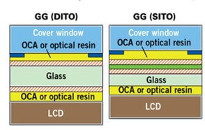
The red shadow in the image above indicates the ITO layer
DITO structure
Apple holds a patent on one DITO construction. DITO offers lower cost. For products sold internationally, check the patent position with counsel before choosing DITO.
SITO structure
SITO does not mean there is only a single ITO layer. It can also have multiple ITO layers. For example, in the case below, it is a SITO structure but includes two ITO layers (and it can have even more). The transmitter (Tx) and receiver (Rx) electrodes can be implemented on the same layer or on different layers, and there can also be additional jump/bridge layers.
Below is the 3D image show the SITO structure:
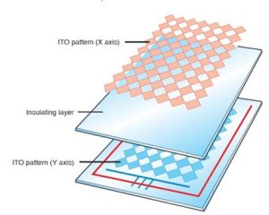
For a SITO design, both X and Y electrodes are implemented on a single ITO layer
SITO integrates both Tx and Rx electrodes on the same surface, which requires careful pattern design and layer management to ensure proper electrical isolation while maintaining stable capacitive coupling. In practice, SITO does not imply a single ITO layer; multiple conductive layers can be implemented on the same side by introducing insulating layers in between, allowing Tx and Rx to be arranged either on the same layer or on different stacked layers.
Bridges and jumpers in SITO
To achieve routing without electrical interference, additional structures such as bridges or jumpers are often used, enabling signal lines to cross over one another within a compact layout.
See below:
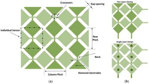
On the left, each diamond-shaped electrode represents an individual sensing unit, with the Tx and Rx electrodes arranged in an interleaved pattern through these diamond structures. Since all electrodes are located on the same side, direct routing would inevitably lead to signal lines blocking or intersecting each other. This is where the crossover structure becomes necessary. The positions labeled “crossovers” in the diagram are typical bridge points.
A bridge (or jumper) essentially works by locally elevating one signal line to cross over another. In practice, this is achieved by first forming a routing line on the bottom ITO layer, then covering it with a dielectric (insulating) layer, and subsequently adding a short conductive bridge on top (which can be made of ITO or metal). This allows the signal to “pass over” the other line before returning to the original layer. By separating the lines vertically in this way, electrical shorting is avoided.
Compared with DITO, SITO may offer more design freedom where patents are a concern; however, it comes with increased process complexity, placing higher demands on alignment accuracy, dielectric uniformity, and yield control of bridge structures, while also requiring careful optimization between optical performance and electrical characteristics.
On the right, DITO can be understood as a structure in which the Tx and Rx electrodes are physically separated onto two different sides of the substrate, typically on opposite surfaces of the glass. In the “Two Layers Design” illustration, this separation is conceptually similar: the electrodes are distributed across different layers, so routing conflicts are inherently avoided.
Unlike SITO, where all electrodes share the same side and require bridge or jumper structures to cross over one another, DITO achieves this separation naturally by placing one set of electrodes (for example, Tx) on the top surface and the other set (Rx) on the bottom surface. As a result, there is no need for local crossover structures, since the signal lines do not compete for space within the same plane.
This architecture simplifies the pattern design and reduces process complexity related to bridge formation, dielectric deposition, and alignment of multi-layer routing on a single side. It also improves electrical performance consistency, since there are fewer discontinuities such as bridge transitions. However, DITO requires double-sided processing, including alignment between the two surfaces of the glass, which introduces its own manufacturing challenges.
If you have any questions, please contact our engineering.
Frequently asked questions
What is the difference between SITO and DITO touch panels?
Does SITO mean there is only one ITO layer?
What is a bridge or jumper in a SITO design?
Why choose SITO over DITO?
What are the trade-offs of a DITO design?
New engineering articles by email.
Keep reading
Resistive vs Capacitive Touch
Design and IntegrationOptical Bonding Explained
Design and IntegrationCover Glass and Surface Treatments
Touch PanelsCapacitive Touch Screens in Deep Water: Comprehensive Analysis of Water & Saline Resistance Design
Touch PanelsThe Evolution of Curved Touch Screens in Automotive Cockpits: From Aesthetics to True Flexibility
Touch PanelsFPC Capacitive Key: A Simple Way to Think About Touch
Have a display project in mind?
Talk to an engineer about the display your application needs.