
Displays

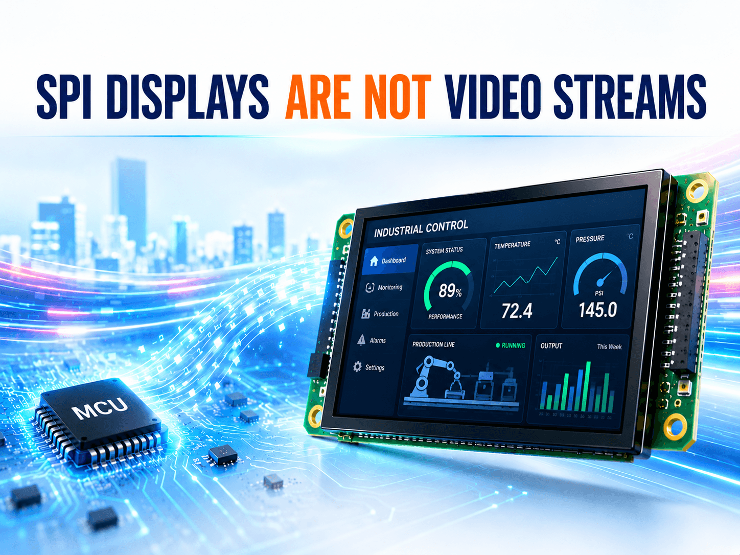
SPI Displays Are Not Video Streams: Understanding Command Mode LCDs

SPI Command Mode LCDs: The Day I Realized Most “SPI Displays” Aren’t Really Streaming Video

When I first started working with embedded displays, I always believed I was using a “pure SPI display.” The MCU continuously sent data through SPI, the screen updated in real time, and from the outside it looked exactly like video streaming. But after digging deeper into how LCD controllers actually work, I realized something important:

Most so-called “SPI displays” are not true streaming displays at all. They are actually Command Mode Displays with internal memory.

And honestly, that realization completely changed how I think about embedded display systems.


What Is an SPI Command Mode Display?

An SPI Command Mode LCD is a display where the MCU sends commands and image data through SPI, while the display controller itself handles the actual screen refreshing.

The key reason is simple:

The display driver IC contains internal frame memory, usually called GRAM (Graphics RAM). Once image data is written into GRAM, the display controller continuously refreshes the panel automatically. The MCU only updates the content when something changes.

In other words:

  • MCU updates the image
  • The display handles the refreshing

The MCU does not continuously “feed” the display.


Why These Displays Are So Popular

SPI command displays are extremely common in embedded systems because they simplify both hardware and software design. They offer several major advantages:

Lower Pin Count

SPI interfaces typically require only a few signals:

  • MOSI
  • MISO
  • SCK
  • CS
  • DC

Compared to RGB interfaces, routing is much simpler and connectors can be much smaller.

Lower EMI

SPI uses serial communication with relatively low bandwidth compared to parallel video interfaces. That usually means:

  • Lower EMI
  • Easier EMC design
  • Better suitability for industrial and medical products

Partial Refresh Support

This is one of the biggest advantages. Instead of refreshing the entire screen, the MCU can update only the region that changes.

For example:

  • Updating the whole screen may require over 100 KB of data
  • Updating only several digits may require just a few KB

That significantly reduces bandwidth and power consumption.


Real-World Embedded Products

Many modern embedded display modules are built around command-mode display architectures with internal GRAM.

For example, our P Series SPI display modules use SPI command interfaces together with onboard display controllers, making them suitable for industrial HMIs, medical devices, handheld devices, and other embedded systems where low EMI and partial refresh are important.

Some products simplify the architecture even further. Our AGN/AGU UART display modules allow the host MCU to communicate through high-level UART commands, while the display module internally handles rendering, framebuffer management, and screen refreshing. This significantly reduces MCU workload and simplifies embedded software development.

We also provide ACN series MCU-interface display modules, which are designed for embedded systems requiring direct MCU communication together with command-based display control architectures.

In many cases, developers are not directly driving LCD pixels at all. They are simply updating display content while the display controller manages the actual refresh process internally.


Why SPI Feels Like Video Streaming

This misunderstanding is actually very common. I had it myself for years. And honestly, it makes perfect sense.


  1. SPI Looks Continuous

SPI can transfer data very quickly.

In many projects, we continuously send image data through SPI, sometimes even refreshing the full screen repeatedly.

Visually, it feels exactly like streaming video.


  1. The Name “SPI Display” Is Misleading

People constantly say things like:

  • SPI LCD
  • SPI display
  • SPI screen

The focus is always on the communication interface, not the display architecture itself. So naturally, many engineers unconsciously assume: SPI = directly driving pixels in real time; But actually: SPI is only the transport method.

The display mode is a completely separate concept.


  1. Driver Libraries Hide the Commands

In application code, we often write something simple like:

LCD_DrawImage(…);

But underneath that function, the driver is actually:

  • Setting display windows
  • Configuring GRAM addresses
  • Sending commands
  • Starting memory writes

All of this is heavily abstracted away.

So over time, it feels like:

“I’m just continuously sending image data.”

Even though the display is actually operating in command mode the entire time.


  1. We Are Updating Memory, Not Driving Pixels

This was the biggest mental shift for me.

Most SPI displays internally store image data inside GRAM.

What we are really doing is:

Writing image data into the display’s internal framebuffer. The display controller then takes care of refreshing the panel itself. That is fundamentally different from true video streaming.

And because this process is mostly invisible to developers:

  • We never see the refresh timing
  • We do not manage line scanning
  • The image remains even after SPI stops

It creates the illusion that we are directly driving the panel. But we are not. We are simply updating what the display should show.


Command Mode vs Video Mode

The core difference is actually very simple.

Command Mode Video Mode
Internal GRAM exists Little or no framebuffer
Display refreshes automatically Continuous pixel stream required
MCU updates when needed MCU continuously outputs frames
Partial refresh supported Usually full-frame streaming
Image remains after communication stops Display stops without input

Typical command-mode interfaces:

  • SPI
  • MCU/8080 interfaces

Typical video-mode interfaces:

  • RGB Parallel
  • LVDS
  • MIPI DSI Video Mode


The Most Important Realization

Eventually I realized something very important:

I was never truly driving pixels in real time.
I was only updating what the display should show.

The display itself was handling the refreshing all along.

And once I understood that:

  • Bandwidth calculations made more sense
  • Partial refresh became intuitive
  • EMI behavior became easier to understand
  • MCU optimization became much clearer

Many embedded display design decisions suddenly stopped feeling mysterious.


Final Thoughts

Looking back, this misunderstanding is incredibly common because several factors combine together:

  • SPI visually resembles streaming
  • Full-screen refreshes imitate video behavior
  • Driver libraries hide the commands
  • Internal GRAM is invisible to developers
  • “SPI display” terminology is misleading

So, it becomes very natural to assume:

“SPI displays are continuously streamed displays.” But in reality, most of them are better understood as: A display terminal with built-in memory.

And honestly, once you realize that difference, you start thinking about embedded displays in a completely different way.


If you have questions or would like to explore your next design, please contact our engineering.

author-avatar

About Veronica Chen

Orient Display - Technical Support

Displays

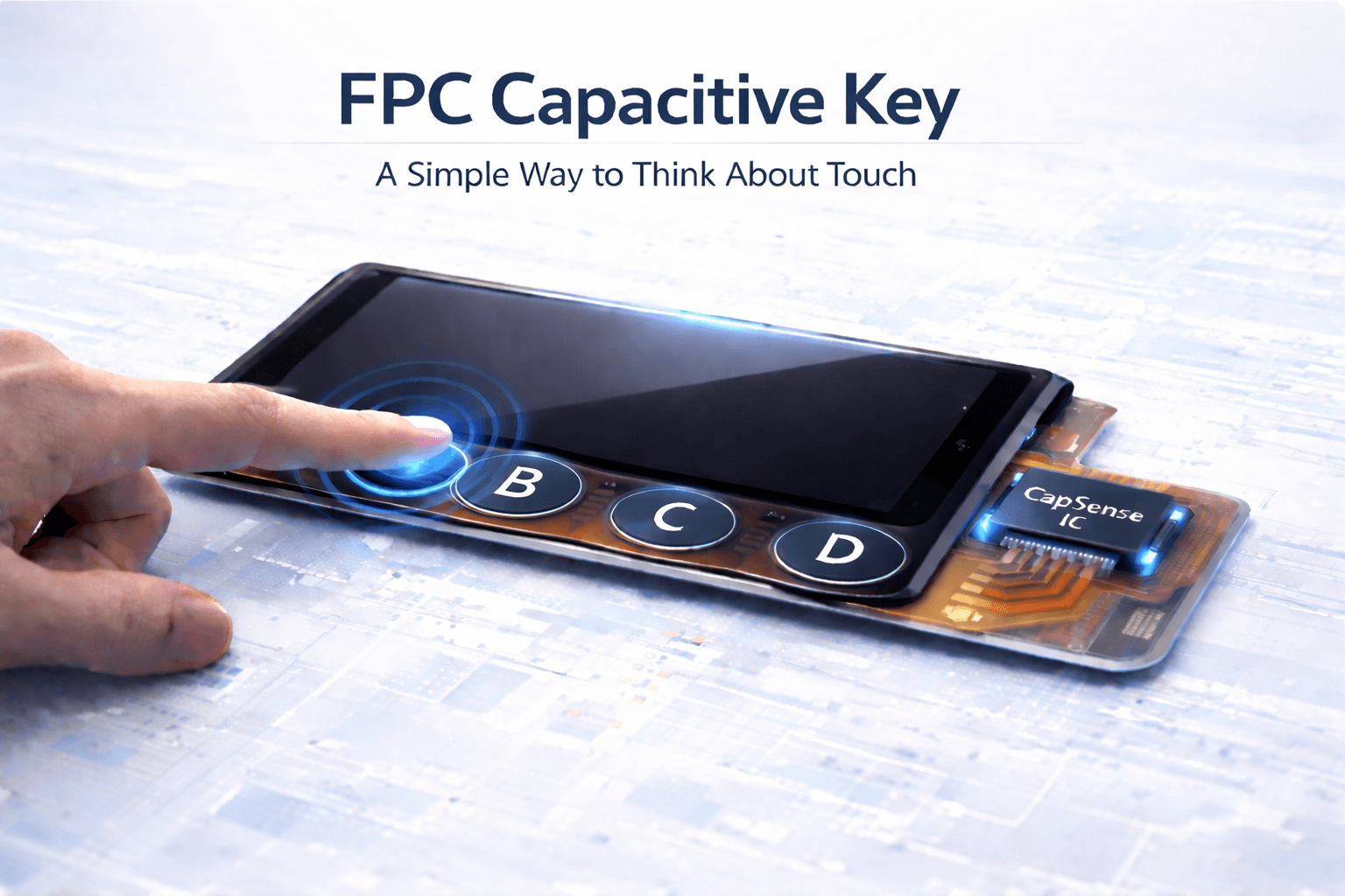
FPC Capacitive Key: A Simple Way to Think About Touch

Sometimes when I look at the touch solutions we use every day, I get the feeling that a lot of designs exist simply because “that’s how it’s usually done,” not because they’re the only option.

Take touch screens, for example.

In most cases, when we say “touch,” we immediately think of a full capacitive touch panel—an entire surface that responds to input anywhere. It works, it’s intuitive, and for many applications, it’s absolutely the right choice.

But when the interaction is limited to just a few buttons, that kind of solution can feel a bit… heavy.


Not All Touch Needs Coordinates

The most common structure we deal with looks something like this:

Cover Lens + OCA + ITO Glass + FPC + Touch Controller

Its job is straightforward: detect where you touch (X-Y coordinates)

This makes perfect sense for interfaces that involve gestures, swiping, or dynamic UI, but not every interaction needs location tracking. Sometimes, all you really need is a simple “trigger.”


A Different Approach: CapSense

This is where capacitive sensing (CapSense) comes in. Instead of tracking position, it detects whether a specific area is being touched.

Typical structure:

Cover Lens + ITO Key (single layer) + FPC + CapSense IC

It’s commonly used for:

  • Buttons
  • Sliders
  • Fixed touch zones

Compared to full touch panels, it simplifies things—but it still relies on ITO.


Taking It One Step Further: Removing ITO

And then there’s an even simpler approach.

FPC Capacitive Key is based on a very straightforward idea:

Replace ITO electrodes with copper electrodes on FPC

Which brings the structure down to:

Cover Lens + FPC + CapSense IC

No ITO layer, no full touch stack. Just what’s necessary.


What It Actually Looks Like

Below is a simplified layout that helps visualize how this approach is implemented.

The display sits in the center; Capacitive keys are distributed around the edges; All key electrodes are routed through the FPC; Each key (A/B/C/D) corresponds to an independent sensing area.

What’s interesting here is that the display and touch inputs are no longer part of the same stack. They coexist—but remain structurally independent.


How It Works

There’s no mechanical action involved, and nothing visibly moves.

  1. Metal electrodes (copper or silver) are formed on the FPC
  2. A sensing IC continuously monitors capacitance
  3. A finger approaches → capacitance changes
  4. The IC detects it and outputs a signal

It feels less like “pressing a button” and more like being detected.


Structurally, It’s Very Simple

From a hardware perspective, the simplicity stands out:

  • Substrate: PET or PI (typically 0.1–0.3 mm)
  • Electrodes: flexible in shape (round, bar, custom)
  • Connection: direct FPC to mainboard
  • Surface: glass or plastic overlay

And one key difference: No need for full ITO film or ITO glass. That alone can open up room in both design and cost.


Manufacturing Is Fairly Straightforward

Typical approaches include:

  • Etching copper electrodes directly on FPC
  • Printing conductive paste (silver or copper)
  • Laminating a protective cover (glass or plastic)
  • Connecting via standard FPC connectors

It feels closer to circuit design than display module integration.


What Stands Out in Practice

After working with this approach, a few characteristics become quite noticeable:

  • No mechanical wear, No pressing action means longer lifespan
  • Flexible form factor, FPC allows bending and tighter layouts
  • Easier sealing, Better suited for waterproof or dustproof designs
  • Simpler structure, Works well as a standalone input module


Where It Has Limits

Of course, it’s not meant to replace everything. Some practical constraints:

  • Sensitive to environment (moisture, gloves, ESD) → requires tuning
  • Larger button areas may reduce responsiveness
  • Requires a dedicated capacitive sensing IC
  • Not transparent

That last point is easy to overlook:

Since there’s no ITO, it doesn’t support transparent or semi-transparent designs


A Simple Way to Think About It

If you strip it down to function:

  • Full interaction interface → use a touch panel
  • Fixed input zones → capacitive keys
  • Prefer a simpler structure → FPC Capacitive Key is worth considering

In the end, it’s not about choosing the most advanced solution. It’s about choosing something that fits—just enough, not more.

And sometimes, making things lighter is already an improvement.


If you have any questions, please contact our engineering.

author-avatar

About Veronica Chen

Orient Display - Technical Support

Displays

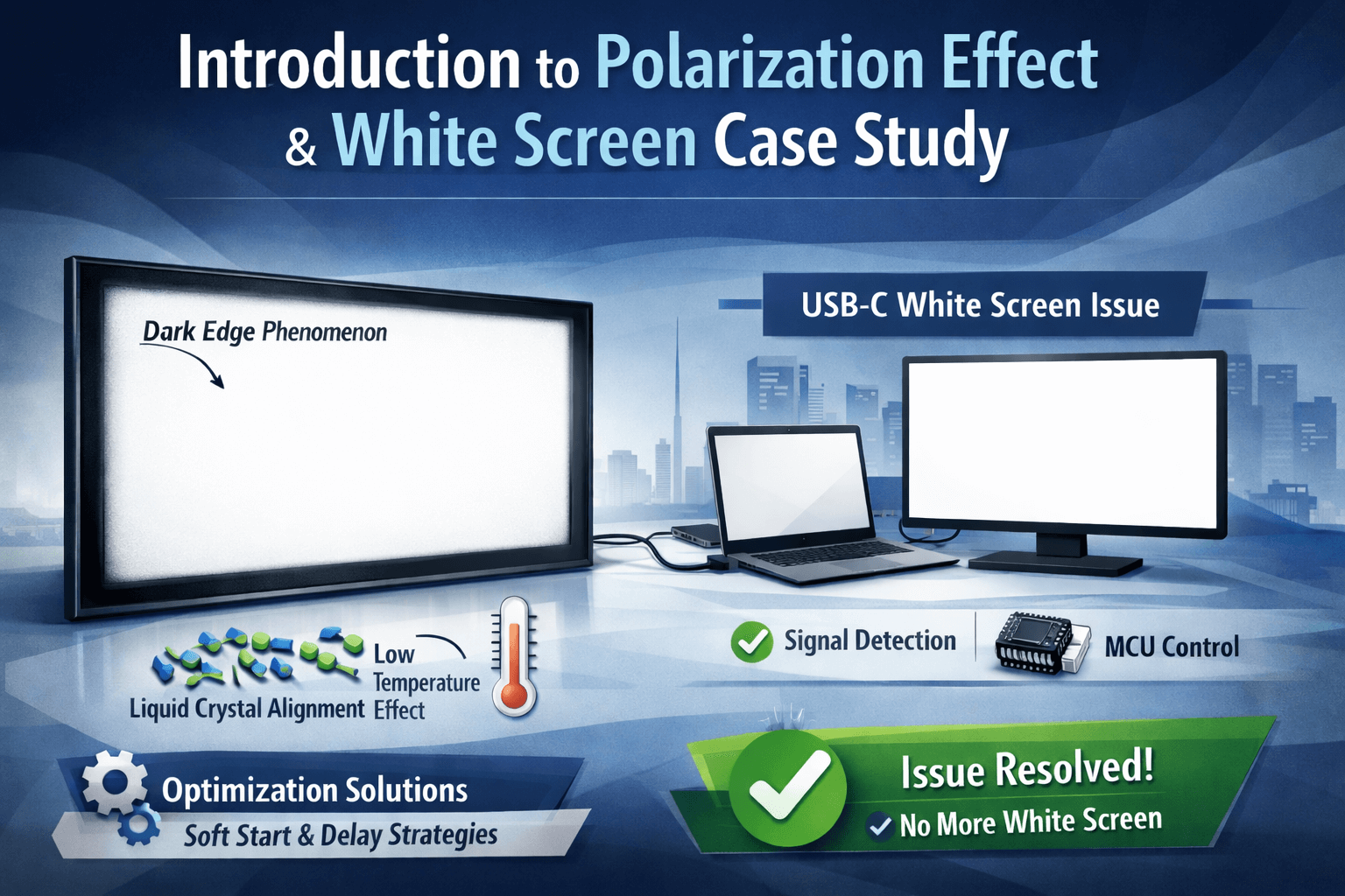
Introduction to Polarization Effect & White Screen Case Study

Brief Introduction to the Polarization (Dark Edge) Phenomenon

Previously, we encountered a phenomenon where, before the LCD fully powers on, a noticeable dark or black border appears around the edges of the screen.

We generally refer to this as a polarization phenomenon. It appears similar to the illustration below.

Characteristics of This Phenomenon

  • Occurs only during initial power-on or cold start
  • Most noticeable under full white or light-colored backgrounds
  • Gradually disappears as the panel temperature rises during operation
  • Does not affect display functionality
  • Does not affect touch performance
  • Does not impact panel lifetime

The dark border typically fades within a few seconds to several tens of seconds.

This is a normal optical characteristic of LCD panels, not a defect and not a quality issue.


Root Causes of the Dark Edge Phenomenon

When the LCD is first powered on, the liquid crystal molecules, voltage driving system, and backlight system have not yet reached a stable operating state. This causes slightly reduced brightness in edge areas, forming a visible dark border.

  1. Initial Polarization of Liquid Crystal

At power-on:

  • Liquid crystal molecular alignment is not fully established
  • Vcom (common voltage) waveform is not yet fully stabilized
  • Positive/negative polarity switching has not fully entered steady-state

The edge area is more sensitive to voltage variations due to:

  • Seal glue (frame seal)
  • Black Matrix (BM) limitations

Under a white background, the edges therefore appear darker than the center.

  1. Low Temperature Effects

When the LCD temperature is low:

  • Liquid crystal viscosity is higher
  • Response time is slower

Edge areas warm up more slowly due to structural shielding, so brightness recovery is delayed — making the dark border more visible.


  1. Backlight Startup Instability

At initial startup:

  • Backlight LED brightness has not fully stabilized
  • Light guide plate edge illumination is not yet uniform

This results in lower brightness at the edges compared to the center.


  1. Structural Light Absorption

LCD edges inherently include several unavoidable structures:

  • Seal glue (Seal)
  • FPC circuit area
  • Black Matrix masking area (BM)
  • Backlight frame edges

These structures absorb more light during startup, amplifying the dark edge effect.


Solutions / Mitigation Methods

  1. Software Optimization (Highly Recommended)

  • Avoid displaying high-gray or pure white images during the first few seconds after power-on
  • Use dark backgrounds (black / dark blue / dark gray) during startup
    → This almost completely hides the phenomenon
  • Delay full-white display by 1–3 seconds
  • Apply gradual backlight ramp-up (soft start) to improve cold-start edge uniformity

  1. Hardware Optimization (If Further Improvement Is Required)

  • Improve panel preheating strategy
    For example, briefly drive low gray levels at startup to accelerate stabilization
  • Fine-tune Vcom voltage (must be verified per panel specification)
    Helps reduce initial polarization deviation
  • Optimize backlight startup curve
    Allows the light guide plate to reach uniform brightness more quickly


  1. Usage Recommendations

  • Avoid displaying pure white high-brightness images immediately under very low temperature conditions
  • At low temperatures, liquid crystal viscosity increases, making dark edges more noticeable


USB-C Sample White Screen Issue – Analysis & Improvement


  1. Observed White Screen Condition

During testing, another issue was observed:

After testing, the display remained connected to the computer. The computer was powered off, but the power supply remained connected. Under this condition, the display panel turned completely white.

The factory initially suggested this was a polarization phenomenon. However, we believe it is more likely related to power supply, backlight control, or display driver logic.

When the laptop lid is closed, the system may enter sleep or standby mode. Although power remains connected, there is theoretically no video signal. In this condition:

  • The display should go dark
  • The backlight should turn off


  1. First Improvement Verification

To resolve the issue, the engineer routed out a video signal detection pin to determine whether a valid video signal was present.

The logic implemented:

  • When video signal is detected → turn on display power
  • When no signal → cut off display power

Testing showed this method was effective:

  • When the video signal was removed, the white screen did not appear
  • However, during signal restoration, a brief white transition was visible

Since this was only a functional verification, further optimization will be implemented via software:

  • When signal is detected, apply a short delay before powering on the display
  • This avoids the visible white transition


  1. Second Improvement Verification

Based on the first solution, further hardware and software optimizations were implemented.

An external MCU was used to control:

  • Signal arrival detection
  • Display power enable
  • Backlight enable

Only after confirming valid signal arrival does the MCU power on the display and backlight.

Results:

  • When the computer is shut down, the display shows no image
  • The backlight is fully turned off
  • The white screen issue is completely resolved


  1. Minor Startup Backlight Flash Issue

Another minor issue was observed:

When the computer boots up and USB-C first supplies power to the display, the display circuitry is still in reset state. During this moment, the backlight briefly flashes.

Solution:

  • Add a delay circuit stage
  • Stagger the power timing between system reset and backlight enable

This eliminates the brief backlight flash.

The adjusted startup time is approximately 1–2 seconds.


If you have any questions, please contact our engineering.

author-avatar

About Veronica Chen

Orient Display - Technical Support

Displays

Privacy Film Knowledge

Types of Privacy Films

Type Principle Features Typical Applications
Micro-Louver Type Uses micro-louver structures to restrict the light emission angle (e.g., ±30° or ±45°) Mainstream type; clear front view, darkens when viewed from the side Smartphones, laptops, ATMs, car displays, industrial monitors
Polarization Type Uses a polarizer to restrict the light vibration direction Higher cost, slightly lower transmittance; suitable for high-contrast displays High-end industrial displays, medical devices
Diffusion Type Scatters light with micro-particles to reduce side visibility Low cost, modest privacy effect, significant brightness reduction Price-sensitive products
Hybrid Type Combines micro-louver with polarizer or anti-reflection Offers multiple functions: privacy, anti-glare, anti-fingerprint High-end laptops, tablets, car infotainment screens


Currently, we mainly use micro-louver type privacy films. The following structure diagrams illustrate the principle:

The micro-louver layer resembles tiny blinds (spacing only tens of microns) that allow light to pass in a specific direction (vertical or ±30°).

  • Front view: Light passes directly → screen content is clear
  • Side view: Light blocked by louvers → screen darkens or becomes invisible

Typical privacy angles:

  • Horizontal: 30°, 45°, 60°
  • Vertical: Up/down privacy is also possible (used for laptops, ATMs, etc.)

From the third structural diagram (this is an automotive light-controlled privacy film), we can see that there are AG layers on both the top and bottom of the privacy film. This type of structure is commonly referred to as a Double-sided AG Privacy Film.

Features:

  • Double-sided anti-glare (AG): Reduces reflections on both surfaces, improves display visibility, scratch-resistant
  • Privacy protection: Darkens at side angles to prevent viewing by others
  • Surface feel: Fine matte AG texture, good anti-fingerprint performance
  • Applications: Outdoor high-brightness TFT LCDs, car displays, industrial monitors, laptops


Structure of Privacy Film

Privacy films are multi-layer composites. Key layers include the base layer, micro-louver layer, OCA, plus optional layers like hard coating and adhesive layers.

  1. Hard Coating Layer: Scratch-resistant, increases surface hardness (typically 3H–9H)
  2. Base PET Layer: Provides mechanical strength and stability
  3. Micro-Louver Layer: Core privacy structure controlling light direction
  4. Optical Adhesive (OCA): Bonds layers while maintaining optical clarity
  5. Adhesive/Silicone Layer: Allows attachment to the screen surface, can be removed and reapplied without residue


Installation Methods

  • Surface-mounted: Uses silicone or OCA; easy to apply, removable; reduces surface hardness
  • Embedded: Laminated inside the LCD module; higher protection, does not affect surface hardness
  • Magnetic/Clip-on: External, detachable; often used for monitors

In our industry, the simplest approach is to attach the privacy film directly to the display surface:

  • Pros: easy, low cost
  • Cons: reduces surface hardness
    Another method is to insert the film between the backlight and LCD glass:
  • Pros: preserves surface hardness
  • Cons: adds to assembly complexity


Key Parameters of Privacy Film

Privacy film parameters fall into four categories: optical, physical structure, environmental/ durability, and surface functions.

  1. Optical Parameters:

  • Visible Light Transmittance (VLT): Ratio of visible light passing through; higher value → brighter screen.
    • Typical range: 50%–85%
  • Viewing Angle / Privacy Angle: Screen is clear at center, darkens beyond this angle.
    • Typical range: ±30°, ±45°, ±60°
  • Haze: Degree of light scattering; higher haze reduces glare but slightly lowers clarity.
    • Typical range: 2%–15% (AG surface)
  • Reflectance: Surface reflection rate; affects anti-glare performance.
    • Typical range: 1%–10%
  • Polarizer Compatibility: Must match TFT LCD polarizer to avoid distortion or color shift
    • Typical range: To Be Verified by Testing

Optical parameters are our main focus. The following are the specifications for the double-sided anti-glare privacy film:

  • Total Light Transmittance: ~70%–80% (high-transmittance privacy film); e.g., a 1000 nits display may drop to 700 nits
  • Transmittance: 70%–80% indicates a high-transmittance privacy film.
  • Haze: 10%–40% clearly shows that the surface has been treated with AG (anti-glare) coating.
  • Up/down (Vertical Viewing Angle) 30° transmittance ≤15%:
    • Up/down 30° angle (±30°): Refers to the viewing angle 30° above or below the vertical center of the screen (vertical privacy direction).

At this angle, visible light passing through the privacy film is less than 15% of the front brightness.

This indicates that the film provides vertical (up/down) privacy protection.

  • Transmittance <15%: At this angle, the intensity of visible light passing through the privacy film is less than 15% of the front-facing brightness.

This means that the privacy film provides vertical (up/down) privacy protection.

Item Unit Typical Value Testing Standard
Thickness of Functional Layers µm 370±20 GB/T 33399
Total Light Transmittance % ≥70 GB/T 2410
Haze º 10~40 GB/T 2410
Transmittance at 30°

Vertical Viewing Angle

% ≤15 /


PS: The table below shows the characteristics of privacy films with different Transmittance levels. This is also helpful for our selection process.

Type Transmittance (Approx. Range) Features
Standard HD Film 90%–95% Clear display, minimal brightness loss
Privacy Film (Standard) 50%–70% Noticeable viewing angle limitation, screen slightly darkened
High-Transmittance Privacy Film 70%–80% Maintains privacy while minimizing brightness loss
Strong Privacy Film 40%–55% Strong privacy effect, but darker screen and deeper colors


  1. Physical / Mechanical Parameters

  • Total Thickness: Overall thickness including PET substrate, AG layer, privacy layer, etc.
    Typical range: 0.1–0.5 mm
  • Base Material: PET, PC, PMMA, Glass Composite, etc.
    Typical range: Depends on application
  • Surface Hardness: Scratch resistance, usually expressed in pencil hardness (H)
    Typical range: 3H–9H
  • AG Layer Roughness (Ra): Affects haze, feel, and anti-reflection performance
    Typical range: 0.02–0.1μm
  • Adhesive Type: Silicone, OCA, or adhesive-free electrostatic


  1. Durability / Environmental Tests

  • Operating / Storage Temperature Range: Typically -20℃ to +80℃
  • Humidity Resistance: No bubbling or discoloration after 60℃ / 90% RH test
  • UV Resistance: No yellowing after prolonged exposure
  • Adhesion Strength: Strength of adhesive bonding to the screen


  1. Surface Treatments / Functionalities

  • Anti-Glare (AG): Reduces reflection, improves outdoor readability
  • Anti-Fingerprint (AF): Oleophobic/hydrophobic, easy to clean
  • Anti-Scratch: Enhances wear resistance
  • Anti-Reflection (AR): Improves optical contrast
  • Anti-Static: Prevents dust attraction


The table below shows how to evaluate or select different types of privacy films based on their parameters.

Dimension Micro-Louver Polarization Diffusion Hybrid
Viewing Angle Clearly specified ±30° / ±45° Smooth decay curve Not specified, only “blurred” Both ± angles + polarizer transmittance data
Transmittance (Tt) 60–75% (relatively high) 35–50% 50–70%, haze > 60% 40–60% (depends on structure)
Haze 10–25% 20–40% 60–90% 30–60%
Contrast Retention ≥90% (front view) ~80% <70% 70–90%
Thickness / Layers 0.25–0.4 mm, double or triple layer ~0.2 mm, with polarizer <0.2 mm, single or double layer >0.4 mm, multi-layer stack
Microstructure Feature Visible parallel micro-groove array No micro-grooves, anisotropic film Rough matte Micro-grooves + polarizer layers

Should you have any questions about privacy film, please consult our engineering.

author-avatar

About Veronica Chen

Technical Support - Orient Display

Displays

Overview of Methods for Driving LED Backlight

1. Operating Principle of LEDs

Before designing a driver circuit, it is important to understand how an LED operates. The brightness of an LED is primarily determined by its forward voltage (VF) and forward current (IF). The current–voltage characteristic curve is shown in Figure 1. Here, VF represents the forward voltage drop, while IF is the forward current.

Once the applied forward voltage exceeds the threshold level (also known as the turn-on voltage, approximately 1.7 V in this case), IF can be considered nearly proportional to VF. As illustrated in the figure, the maximum forward current of an LED can reach up to 1 A, while the typical forward voltage range is about 2 V to 4 V.


Figure 1. Relationship between VF and IF

The forward voltage drop of an LED can vary over a relatively wide range (more than 1 V). From the VF–IF curve shown above, it is clear that even a small change in VF can cause a large variation in IF, which in turn leads to significant fluctuations in brightness. For this reason, the luminous characteristics of LEDs are generally described as a function of current rather than voltage.

However, in typical rectifier circuits, the output voltage fluctuates with changes in the mains supply voltage. This means that using a constant-voltage source cannot ensure consistent LED brightness and may negatively affect LED performance. Therefore, LED drivers are usually designed to operate as constant-current sources.

2. LED Driving Techniques

From the operating principle of LEDs, it is clear that to maintain optimal brightness, an LED must be driven by a constant-current source. The driver’s role is not only to ensure this constant-current characteristic but also to achieve low power consumption.

To meet these requirements, the commonly used methods of current control include:

  • Adjusting the value of a current-limiting resistor to regulate the current.
  • Varying the reference voltage across the current-limiting resistor to control the current.
  • Using PWM (Pulse Width Modulation) to achieve current regulation.

The techniques employed in LED drivers are very similar to those used in switch-mode power supplies. In essence, an LED driver is a type of power conversion circuit, but its output is a constant current rather than a constant voltage. Under all conditions, the circuit must deliver a stable, average current, with ripple current kept within a specified range.

(1) Current-Limiting Method
Figure 2 shows the simplest circuit that uses the current-limiting method.


Figure 2. Simplest Circuit of the Current-Limiting Method

As shown in Figure 3, this is the traditional circuit configuration. The mains voltage is stepped down, rectified, and filtered, then a series resistor is used for current limiting to keep the LED operating stably and to provide basic protection.

However, the fatal drawback of this approach is that the power dissipated in the resistor R directly reduces system efficiency. Combined with transformer losses, the overall system efficiency is only about 50%. Moreover, when the supply voltage fluctuates within ±10%, the current through the LED can vary by 25% or more, and the power delivered to the LED may change by over 30%.

The main advantage of resistor current limiting is its simplicity, low cost, and lack of electromagnetic interference (EMI). Nevertheless, its disadvantages are significant: the LED brightness changes with variations in VF, the efficiency is very low, and heat dissipation becomes a serious issue.

Figure 3. Traditional Resistor Current-Limiting Circuit

There is also a straightforward article online about the current-limiting method that can be referenced: https://www.ourpcb.com/current-limiting-resistor.html

For more information on constant-current LED backlight driving, see: https://orientdisplay.com/wp-content/uploads/2018/07/OrientDisplay-Backlight-Constant-Current-Driver.pdf

(2) Voltage Regulation Method
As shown in Figure 4, this circuit is based on Figure 3, with the addition of an integrated voltage regulator (MC7809). This keeps the output voltage essentially stable at 9 V, allowing the current-limiting resistor R to be made very small, which prevents voltage instability across the LED.

However, the efficiency of this circuit remains low. Since the voltage drop across both the MC7809 and resistor R1 is still significant, the overall efficiency is only about 40%. To achieve both stable LED operation and higher efficiency, low-power current-limiting components and circuits should be used to improve system performance.

The linear voltage regulation method has the advantages of simple structure, few external components, medium efficiency, and relatively low cost.

Figure 4 Voltage Regulation Method

(3) PWM Method
PWM (Pulse Width Modulation) controls LED brightness by adjusting the duty cycle of the driving current pulses. This dimming technique repeatedly switches the LED driver on and off using simple digital pulses. By supplying digital pulses of varying width, the output current can be modulated, thereby changing the brightness of a white LED.

The distinctive feature of this driving circuit is that energy is transferred to the load through an inductor. Typically, a PWM control signal is used to switch a MOSFET transistor on and off. By varying the duty cycle of the PWM signal and the charging/discharging time of the inductor, the ratio between input and output voltage can be regulated.

Common circuit topologies of this type include buck, boost, and buck–boost converters. The advantages of the PWM method are high efficiency and stable performance, but its drawbacks include audible noise, higher cost, and more complex design.

Figure 5. LED Driving Circuit Using PWM Method

As shown in Figure 5, the PWM signal is connected through the base of transistor VQ1 to the gate of a P-channel MOSFET. The gate of the P-channel MOSFET is driven by a simple NPN transistor amplification circuit, which improves the MOSFET’s conduction process and reduces the power consumed by the driver circuit.

If the MOSFET is driven directly by the circuit, the rapid switching on and off of the MOSFET can cause oscillations in the drain–source voltage. This may lead to radio frequency interference (RFI) and, in some cases, expose the MOSFET to excessively high voltages, resulting in breakdown and damage.

To address this problem, a non-inductive resistor is inserted in series between the gate of the driven MOSFET and the driver circuit output. When the PWM signal is at a high level, transistor VQ1 conducts, pulling the MOSFET gate voltage below the source voltage. As a result, the MOSFET turns on, and the LED lights up. Conversely, when the PWM signal is at a low level, VQ1 is cut off, the MOSFET turns off, and the LED is extinguished.

3. LED Driver IC Solutions

LED backlight driver ICs are primarily used in LCD displays (televisions, laptops, mobile phones, automotive screens, etc.) to provide a constant current or constant voltage to the LED modules. Their purpose is to ensure uniform brightness, high efficiency, and long lifetime. Common driver topologies include boost (step-up), buck (step-down), buck–boost, and multi-channel constant-current drivers. Below are several representative categories of LED backlight driver ICs:

(1). Texas Instruments (TI)

  • TPS61169: Single-channel boost constant-current driver, suitable for small-size LCDs (e.g., mobile phones).
  • LP8556: Supports I²C control, multi-channel output (up to 6 channels), and both PWM/analog dimming. Widely used in laptops and automotive displays.

(2). ON Semiconductor (now onsemi)

  • NCP3170 / NCP3170B: High-efficiency buck drivers, suited for small- to medium-size screens.
  • NCV7685: 16-channel constant-current driver, often used in automotive backlighting and dashboards, featuring high reliability and diagnostic functions.

(3). STMicroelectronics (ST)

  • STLED524: Multi-channel LED backlight driver with I²C interface.
  • L5973D: Boost DC-DC converter for medium-power LED backlight systems.

(4). Renesas Electronics

  • ISL98611: Integrates boost and positive/negative charge pump outputs, designed for smartphone power and backlight driving.
  • ISL97900: Multi-channel LED backlight driver with high-precision current matching.

(5). China Manufacturers

  • Macroblock (MBI series): e.g., MBI5030, focused on large-display and backlight drivers, widely used in TVs and advertising panels.
  • Solomon Systech: Has released LED backlight driver solutions for mobile phones and small-to-medium displays.
  1. Summary
  • Small-size screens (phones, tablets): TI TPS/LP series, Renesas ISL series.
  • Medium-to-large screens (laptops, monitors, TVs): Multi-channel constant-current drivers such as TI LP8556, ST STLED524, Macroblock MBI series.
  • Automotive and industrial applications: Require reliability and multi-channel control, typically using onsemi NCV series.

4. Comparison Table of LED Backlight Driver ICs

Manufacturer Model Channels Driving Method Control Interface Typical Applications
TI (Texas Instruments) TPS61169 Single-channel Boost constant-current PWM / Analog Mobile phones, small displays
TI LP8556 6 channels Multi-channel constant-current with boost I²C + PWM Laptops, automotive displays
onsemi (formerly ON Semiconductor) NCP3170 Single-channel Buck constant-current PWM Small- to medium-size screens
onsemi NCV7685 16 channels Constant-current SPI / I²C Automotive backlight, dashboards
ST (STMicroelectronics) STLED524 6 channels Multi-channel constant-current I²C Monitors, televisions
ST L5973D Single-channel Boost DC-DC constant-current PWM / Analog Medium-power backlight
Renesas ISL98611 3 channels + power outputs Boost + charge pump I²C Smartphones, tablets
Renesas ISL97900 Multi-channel Constant-current I²C Laptops, tablets
Macroblock (明微电子) MBI5030 16 channels Constant-current SPI TVs, large advertising displays
Solomon Systech (晶门科技) SSD series (e.g., SSD2805) 6–8 channels Multi-channel constant-current I²C Mobile phones, small-to-medium displays

5. Key Parameter Comparison of LED Backlight Driver ICs

Manufacturer Model Input Voltage Range Output Channels Max Current (per channel) Efficiency Package Typical Applications
TI TPS61169 2.7–18 V 1 1.2 A ~90% SOT-23 Mobile phones, small displays
TI LP8556 2.7–5.5 V 6 30 mA ~90% WQFN Laptops, automotive displays
onsemi NCP3170 4.5–18 V 1 3 A ~90% SOIC-8 Small- to medium-size screens
onsemi NCV7685 6–40 V 16 75 mA ~85% TSSOP Automotive backlight, dashboards
ST STLED524 2.7–5.5 V 6 30 mA ~85–90% QFN Laptops, monitors
ST L5973D 4–36 V 1 2 A ~90% HSOP-8 Industrial / medium-power backlight
Renesas ISL98611 2.5–5.5 V 3 + power rails 30 mA ~90% WLCSP Smartphones, tablets
Renesas ISL97900 2.5–5.5 V 6 25 mA ~90% QFN Laptops, tablets
Macroblock MBI5030 3–5.5 V 16 80 mA ~85% SSOP/QFN Large TVs, advertising panels
Solomon Systech SSD2805 2.7–5.5 V 6–8 25 mA ~85% QFN Mobile phones, small-to-medium displays


Key Comparison Points

1.      Number of Channels

o   Small screens → Single-channel (e.g., TPS61169)

o   Medium screens / Automotive → 6-channel (e.g., LP8556, STLED524)

o   Large screens / Televisions → 16 channels or more (e.g., NCV7685, MBI5030)

2.      Driving Method

o   Boost (step-up) → Common in smartphones and tablets, used to raise low supply voltages to higher levels for driving multiple LEDs in series.

o   Buck (step-down) → Better suited for high-voltage power sources driving fewer LEDs.

o   Multi-channel constant-current → Ensures brightness uniformity, ideal for large-screen backlighting.

3.      Control Interface

o   PWM → Simple, widely used in mobile devices.

o   I²C → More flexible, allows adjustable current, voltage, and dimming curves.

o   SPI → High-speed and multi-channel, well-suited for TVs and advertising displays.


6. Recommended Application Scenarios for LED Backlight Driver ICs

  • Small-size screens (smartphones / tablets) → Single-channel boost drivers, e.g., TI TPS61169, Renesas ISL98611
  • Medium-size screens (laptops / automotive displays) → 6-channel multi-channel constant-current drivers, e.g., TI LP8556, ST STLED524, Renesas ISL97900
  • Large-size screens (monitors / TVs) → 16-channel or higher constant-current drivers, e.g., Macroblock MBI5030
  • Special scenarios (automotive / advertising displays) → High-reliability multi-channel drivers, e.g., onsemi NCV7685, Macroblock MBI series
author-avatar

About Veronica Chen

Technical Support - Orient Display

Displays

UV Protection Methods for Polarizers

Enhancing UV Resistance (100nm ~ 400nm) in Polarizers

Enhancing UV resistance (100nm ~ 400nm) is essential to prevent the polarizer layer from fading, degrading, yellowing, or failing due to ultraviolet exposure. Additionally, UV can damage the molecular structure of liquid crystals, leading to reduced performance. Once liquid crystal materials degrade, color deviation or yellow spots may occur, affecting display uniformity, image quality, and lifespan.

This time, we will focus on how to improve the UV resistance of polarizers.


Understanding Polarizer Structure and Process Flow

To understand how to enhance the UV resistance of a polarizer, we first need a basic understanding of its structure and manufacturing process.


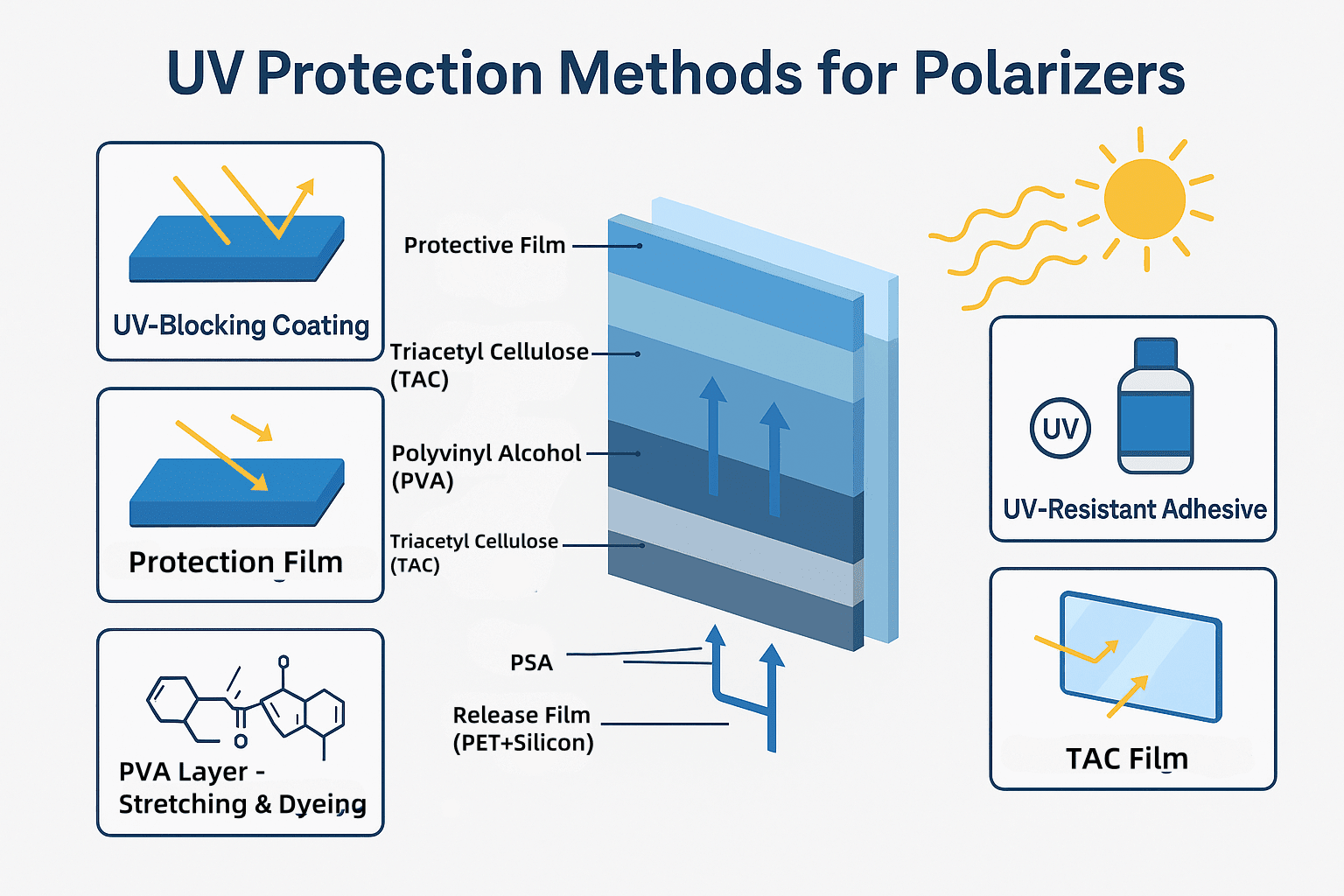
General Structure of a Polarizer:

  1. Surface Coating:
    • Optional additional treatments.
    • Functional coatings applied directly to the surface of the TAC film.
    • Examples: Anti-scratch coatings (used in most polarizers), AR (Anti-Reflective), AF (Anti-Fingerprint), AS (Anti-Smudge), UV-blocking.
  2. Functional Film (Surface Protection Layer):
    • Optional additional film bonded to the TAC surface for enhanced performance.
    • Examples: Brightness enhancement film, UV protection, AF/AR/AS coatings, anti-static film.
  3. TAC Film (Triacetyl Cellulose) – Upper TAC:
    • Provides physical protection and structural support.
    • Protects the polarizer layer from scratches, moisture, oxidation, etc.
    • Offers mechanical strength and flexibility.
  4. PVA Polarizer Layer – Polyvinyl Alcohol:
    • The core functional layer.
    • After stretching, PVA molecules align with dye molecules, which selectively absorb light waves in a specific direction, thus achieving polarization.
  5. TAC Film – Lower TAC:
    • Symmetrical structure enhances mechanical strength.
    • Protects the underside of the polarizer layer.
  6. Pressure-Sensitive Adhesive (PSA) or Optical Clear Adhesive (OCA):
    • Bonds the polarizer to the LCD or touch panel glass.
    • Must remain transparent, bubble-free, and resistant to yellowing.
  7. Release Film or Protective Film

From this structure, it’s clear that the PVA polarizer layer is the most critical component. Therefore, to better understand how to enhance UV resistance, we must also understand the manufacturing process of the PVA polarizer layer.


PVA Polarizer Layer Manufacturing Steps

  • Dyeing:
    PVA is a water-soluble polymer. It is immersed in a solution containing iodine or organic dyes, which adhere to the film to form the polarizing material.
  • Stretching (Orientation):
    The dyed PVA film is stretched in one direction to align the dye molecules. These molecules selectively absorb light waves aligned with their direction, creating linearly polarized light. The transmitted light is perpendicular to the orientation of the dye.
  • Crosslinking Treatment (to enhance water resistance and stability):
    The stretched film is treated with chemical crosslinking agents such as boric acid and sodium ions to increase mechanical strength and moisture resistance.
  • Drying:
    The film is dried to remove excess moisture and stabilize the polarization effect.


Complete Production Flow of a Polarizer

Raw materials → Dyeing → Stretching → Crosslinking → Drying → Lamination → Cutting → Inspection → Packaging


Strategies to Enhance UV Resistance

Several structural and process-related measures can be taken to improve UV resistance:

  1. Surface Coating:

  • Apply UV-curable coatings containing UV protection components or nano UV shielding materials.
  • Provides a durable surface protection layer.
  1. Functional Protection Film:

  • Add UV barrier films (e.g., PET + UV coating) to further block short-wave UV rays.
  1. Upper and Lower TAC Films:

  • Use TAC films with UV absorbers to absorb UV rays (especially in the 280–400nm range), preventing penetration and protecting the internal PVA layer.
  • UV-absorbing or UV-reflecting coatings may also be applied to the TAC surface, especially in high-end applications.
  1. PVA Layer – Dyeing and Stretching:

Stretching Process:

  • During polarizer manufacturing, PVA films are dyed, then stretched to align dye molecules.
  • Unstretched PVA resembles tangled threads (random molecular chains), while stretched films have orderly aligned chains—like neatly combed hair—which control light direction.

How Stretching Enhances UV Resistance:

  1. Molecular Orientation Enhances UV Absorption (Indirect UV Protection):
    • Stretched PVA has highly ordered molecular chains, offering better light stability.
    • If UV-absorbing dyes are used (e.g., iodine-based), stretching aligns them for more effective UV absorption.
    • Even without dye, stretched PVA shows slightly enhanced UV absorption.
  2. Improved Structural Stability and UV Aging Resistance:
    • Stretching increases crystallinity and tightens molecular structure, improving UV durability.
    • Crucial for long-term exposure scenarios (e.g., outdoor sunglasses, automotive displays).
  3. Reduced Free Radical Pathways:
    • UV light excites unsaturated bonds in polymers, forming free radicals that cause degradation.
    • Ordered molecular structures reduce free radical diffusion, improving UV resilience.

Dyeing Process:

  • PVA alone absorbs little visible light—even after stretching—so polarization efficiency is low.
  • Dyes (like iodine) absorb light in specific directions and align with PVA chains during stretching to create high polarization efficiency (high transmission + high polarization).
  • Using UV-resistant, highly photostable dyes (e.g., special anthraquinone or azo dyes) prevents fading and extends lifespan.
  • Dye concentration must be controlled to avoid UV-accelerated degradation from overdosing.

Especially in LCDs, where high polarization performance is required, stretched dye films remain the most cost-effective and high-performance solution.

  1. Adhesive Layer (PSA/OCA):

  • Used to bond the two TAC films and the PVA layer.
  • Must be optically clear and durable.
  • Use optical adhesives with UV inhibitors to prevent yellowing, bubbling, or failure under UV.
  • Uniform coating/lamination without bubbles is critical to avoid UV leakage paths.


Summary: Key Points on UV Resistance in Polarizers

  1. UV radiation is the main external factor causing polarizer aging, especially for the PVA layer and dye structure. It leads to fading, breakage, contrast loss, and reduced display/module lifespan.
  2. UV resistance design involves both materials and structure:
    • Material level: Use TAC films, optical adhesives, and surface coatings with UV absorbers—mainstream absorbers include benzotriazole and triazine compounds.
    • Structural level: Stack UV-cut films or use UV coatings for enhanced shielding—especially critical for outdoor or in-vehicle applications with high UV exposure.
  3. Working principle of UV absorbers:
    • Convert UV energy into heat or harmless long-wave radiation, protecting the core PVA and dye layers from degradation.
    • UV cut performance is reflected in how well the entire structure limits UV (<400nm) transmission.
  4. Surface protection designs also play a key role:
    • Modern polarizers usually include a hard anti-scratch coating (HC).
    • Additional functional films (AR, anti-smudge, UV-blocking) may be added based on application needs vs. cost.
  5. System-level perspective:
    • Polarizers are just one part of the UV protection system.
    • Liquid crystals, light guide structures, and full module sealing are equally important.
    • UV resistance should be considered at the system design stage—for example, adding front-cover UV filter glass, using UV-resistant liquid crystal materials, etc.


Conclusion:

UV resistance is not just the task of a single material, but a multi-layered, multi-material system design strategy that directly affects the long-term stability and reliability of LCD displays.


author-avatar

About Veronica Chen

Technical Support - Orient Display

Displays

The Complete Guide to Display Coatings: How AG, AF, and AR Solutions Solve Critical Display Problems

Why Do Display Coating Problems Cost Businesses Money?

Every day, businesses lose productivity and customer satisfaction due to display readability issues. Outdoor kiosks become unreadable in sunlight. Medical equipment screens create dangerous glare for healthcare workers. Touch devices accumulate fingerprints, which can be frustrating for users and require regular cleaning. Industrial control panels reflect overhead lighting, making critical information difficult to see.

At Orient Display, we’ve engineered coating solutions to help manufacturers solve these exact problems across automotive, medical, industrial, and consumer applications. The right coating choice can mean the difference between a display that enhances user experience and one that creates operational headaches.

What Are AG, AF, and AR Display Coatings?

Display coatings are specialized surface treatments that solve specific visibility and usability problems. The three most effective solutions are:

AG (Anti-Glare) reduces harsh reflections and eye strain by creating a matte surface that scatters light, making displays more comfortable to view under bright lighting.

AF (Anti-Fingerprint) creates an oil and water-repelling surface that prevents fingerprint buildup and makes displays easier to clean, crucial for touch interfaces.

AR (Anti-Reflection) uses optical interference to eliminate mirror-like reflections while maintaining crystal-clear image quality, essential for outdoor and high-brightness applications.

How Do These Coatings Compare for Performance and Applications?

Based on our extensive testing and customer deployments, here’s how these coatings perform across key metrics:

Coating Type Primary Function Surface Appearance Best Applications Key Benefit
AG (Anti-Glare) Reduces harsh glare and eye strain Matte finish with slight texture Indoor displays, office equipment, reading devices Enhanced visual comfort in bright environments
AF (Anti-Fingerprint) Repels oils and fingerprints Smooth, easy-to-clean surface Touch screens, mobile devices, kiosks Reduced maintenance, improved touch experience
AR (Anti-Reflection) Eliminates reflections, increases light transmission Crystal clear, transparent Outdoor displays, automotive, high-end electronics Maximum clarity and contrast in all lighting

Can You Combine Different Coating Types?

Yes, and many applications benefit significantly from combined treatments. Here’s what our engineering experience has shown works best:

Coating Combination Performance Benefits Best Use Cases Trade-offs to Consider
AG + AR Enhanced visual comfort with improved clarity Automotive displays, industrial HMI Slight reduction in sharpness due to AG matte effect
AG + AF Comfortable viewing plus easy cleaning Office equipment, indoor kiosks AF layer must be matched to AG surface texture
AR + AF Maximum clarity with fingerprint resistance High-end smartphones, tablets, premium displays Higher cost but superior user experience
AG + AR + AF Complete protection and performance Medical equipment, luxury automotive, outdoor industrial displays Highest cost and processing complexity

What’s the Best Coating for Outdoor Displays?

For outdoor applications, AR (Anti-Reflection) coating is typically the superior choice for outdoor use scenarios.

Outdoor displays face direct sunlight, which creates intense reflections that make screens unreadable. AR coating provides enhanced clarity and anti-reflection performance. AR coating can significantly improve visibility in bright outdoor conditions.

However, for cost-sensitive outdoor applications, AG coating is often recommended for cost-sensitive outdoor use, providing a reasonable compromise for glare reduction.

Our Recommendation: For applications requiring maximum clarity and outdoor visibility, choose AR coating. For budget-conscious applications, AG provides good value for outdoor glare reduction.

Which Coating Should Automotive Manufacturers Choose?

Automotive displays require the most demanding performance standards due to safety implications and harsh operating conditions. Based on our automotive partnerships, here’s what works:

For Dashboard and Center Console Displays: For automotive and industrial HMIs, we recommend:

  • AG + AR or AG + AR + AF composite treatment provides optimal performance
  • AG reduces glare and relieves visual fatigue
  • AR reduces reflectance and enhances image clarity
  • AF prevents fingerprint buildup that could obstruct critical information

For HUD (Head-Up Display) Applications:

  • AR coating is essential to prevent double imaging
  • Must achieve very low reflectance for optical clarity
  • Requires high-performance AR treatment for durability

What Coating Works Best for Touch Devices?

Touch devices prioritize feel, cleanliness, and visual quality. Here’s our recommended approach:

For Consumer Electronics (Phones, Tablets):

  • AF + AR combination delivers the best user experience
  • AF coating provides a smooth touch feel and fingerprint resistance
  • AR coating maintains display clarity and reduces battery drain from increased brightness compensation

For Industrial Touch Panels:

  • AG + AF combination handles harsh usage patterns
  • AG reduces glare in industrial lighting environments
  • AF coating must withstand frequent cleaning with industrial solvents

How Are These Coatings Manufactured and Applied?

Understanding the manufacturing process helps explain performance differences and cost variations. Here are the primary methods we use:

AG (Anti-Glare) Processing Methods

Chemical Etching (Glass Applications)

  • Process: Acid etching creates microscopic surface irregularities
  • Performance: 88-91% light transmission, 3-6% reflectance
  • Best for: High-durability applications, harsh environments
  • Cost: Medium

AG Film Application

  • Process: Micro-particle resin coating applied to PET film base
  • Performance: 89-93% light transmission, 2-4% reflectance
  • Best for: Cost-effective applications, easy installation
  • Cost: Medium to high

AF (Anti-Fingerprint) Processing Methods

Physical Vapor Deposition (PVD)

  • Process: Vacuum deposition of fluorinated compounds
  • Performance: Contact angle up to 120°, >6H hardness
  • Best for: High-durability, frequent-touch applications
  • Cost: High

Solvent-Based Coating

  • Process: Solution application of fluorosilane compounds
  • Performance: Contact angle 100-115°, moderate durability
  • Best for: Standard consumer applications
  • Cost: Low to medium

UV-Cured Nanocoating

  • Process: UV-polymerized fluoropolymer coating
  • Performance: Contact angle 95-110°, good weather resistance
  • Best for: Outdoor applications, balanced cost/performance
  • Cost: Medium

AR (Anti-Reflection) Processing Methods

Vacuum Thin-Film Coating

  • Process: Multi-layer optical films (MgF₂, SiO₂, TiO₂) deposited in vacuum
  • Performance: <0.5% reflectance, 97-99% transmission
  • Best for: Premium applications requiring maximum performance
  • Cost: High

Sol-Gel Nanocoating

  • Process: Spray or dip application of nanoscale materials
  • Performance: 1-2% reflectance, 96-98% transmission
  • Best for: Cost-effective AR solution
  • Cost: Medium

Moth-Eye Nanostructure

  • Process: Etched nanoscale surface structures
  • Performance: <0.2% reflectance, 98-99% transmission
  • Best for: Ultra-premium applications, wide viewing angles
  • Cost: Very high

How Long Do Different Coating Types Last?

AF film adhesion and service life depend on the substrate and coating technology; it is prone to wear in environments with frequent wiping. Chemical-etched AG glass provides high durability with abrasion resistance, while AG films depend on the coating quality.

Key Durability Factors:

  • Chemical-etched AG: High durability, abrasion resistant
  • AG Films: Durability depends on coating quality
  • PVD AF: Superior adhesion and longevity compared to other AF methods
  • Solvent-based AF: Average durability, prone to degradation
  • Vacuum AR coating: Excellent stability and long durability

Coating durability directly impacts total cost of ownership and should be considered when selecting treatments for specific applications.

How Much Do Different Coatings Cost?

Coating costs vary but does not provide specific cost multipliers. Cost considerations include initial treatment, durability, and maintenance over the product lifecycle. Different processing methods have varying cost implications:

  • Chemical etching: Medium cost
  • AG Film: Medium to high cost
  • PVD AF: High cost
  • Solvent-based AF: Low to medium cost
  • UV-cured AF: Medium cost
  • Vacuum AR: High cost
  • Sol-Gel AR: Medium cost
  • Moth-Eye nanostructure: Very high cost

High-end products often employ AG + AR + AF three-layer composite films or coatings, which have the highest cost and greatest processing difficulty.

What Makes Orient Display’s Coating Solutions Different?

Our 2 decades of display engineering experience mean we understand both the technical requirements and real-world challenges our customers face. We provide comprehensive technical analysis and application-specific recommendations to help you select the optimal coating solution.

Technical Expertise: We offer detailed guidance on coating selection, processing methods, and performance optimization for specific applications across automotive, medical, industrial, and consumer electronics sectors. Our engineering team understands the critical performance requirements for each application type and can recommend the most effective coating combinations for your specific needs.

Contact our engineering team to request a consultation: tech@orientdisplay.com

How Do I Choose the Right Coating for My Application?

Use this decision framework based on your primary requirements:

Step 1: Identify Your Primary Challenge

  • Glare/Eye Strain: Start with AG coating evaluation
  • Fingerprints/Cleaning: Prioritize AF coating solutions
  • Reflections/Outdoor Visibility: Focus on AR coating options

Step 2: Consider Your Environment

  • Indoor/Controlled Lighting: AG or AF coating often sufficient
  • Outdoor/Variable Lighting: AR coating typically required
  • High-Touch Applications: AF coating essential

Step 3: Evaluate Performance Requirements

  • Consumer Products: Balance cost and performance
  • Professional/Industrial: Prioritize durability and reliability
  • Safety-Critical: Choose proven, high-performance solutions

Step 4: Assess Total Cost of Ownership

  • Initial Cost: Compare coating treatment costs
  • Maintenance: Factor in cleaning and replacement costs
  • User Experience: Consider productivity and satisfaction impacts

What Questions Should I Ask When Selecting a Coating Partner?

When evaluating coating suppliers, these questions reveal technical capability and experience:

Technical Questions:

  • What specific coating processes do you control in-house?
  • Can you provide performance data from similar applications?
  • How do you ensure coating uniformity across large displays?
  • What quality control testing do you perform?

Experience Questions:

  • How many similar projects have you completed?
  • Can you provide customer references in my industry?
  • What technical challenges have you solved for similar applications?
  • How do you handle custom coating requirements?

Support Questions:

  • What engineering support do you provide during design?
  • How do you handle performance testing and validation?
  • What documentation and certification can you provide?
  • How do you support field issues or warranty claims?

Ready to Solve Your Display Coating Challenges?

Whether you’re dealing with outdoor readability issues, fingerprint accumulation, or glare problems, the right coating solution can transform your display performance. Our engineering team has solved these exact challenges across thousands of applications.

Next Steps:

  1. Technical Consultation: Share your application requirements with our engineering team
  2. Performance Testing: We’ll recommend optimal coating solutions and provide test samples
  3. Cost Analysis: Receive detailed pricing and total cost of ownership analysis
  4. Production Planning: Integrate coating solutions into your manufacturing timeline

Contact our engineering team: tech@orientdisplay.com

Request a consultation: Share your display specifications, operating environment, and performance requirements for customized coating recommendations.

Orient Display has been engineering custom display solutions with expertise spanning automotive, medical, industrial, and consumer electronics applications. Our coating solutions are deployed in devices worldwide, from automotive dashboards to medical equipment interfaces.

author-avatar

About Veronica Chen

Technical Support - Orient Display

Control Board, Displays

Introduction to Cover Glass for Displays

Cover Glass (Cover Lens) is primarily used as the outermost layer of touch screens. The main raw material for these products is ultra-thin flat glass, which offers features such as impact resistance, scratch resistance, oil and fingerprint resistance, and enhanced light transmittance. It is currently widely used in various electronic consumer products with touch and display functionalities.

1. Classification of Glass

a. Soda-lime glass: Primarily composed of SiO₂, with additional content of 15% Na₂O and 16% CaO.
b. Aluminosilicate glass: Mainly composed of SiO₂ and Al₂O₃.
c. Quartz glass: Contains more than 99.5% SiO₂.
d. High-silica glass: Contains approximately 96% SiO₂.
e. Lead-silicate glass: Mainly composed of SiO₂ and PbO.
f. Borosilicate glass: Primarily made up of SiO₂ and B₂O₃.
g. Phosphate glass: Mainly composed of phosphorus pentoxide (P₂O₅).

Types c through g are rarely used in displays, so they will not be discussed here.

2. Processing Techniques for Glass Raw Materials

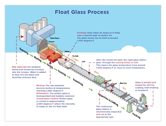
a. Float Glass

Float glass is produced using raw materials such as sea sand, quartz sandstone powder, soda ash, and dolomite. These materials are mixed and melted at high temperatures in a furnace. The molten glass continuously flows from the furnace and floats on the surface of a molten metal bath, forming a uniformly thick, flat glass ribbon that is flame-polished. After cooling and hardening, the glass separates from the molten metal, and it is then annealed and cut to create transparent, colorless flat glass. The forming process of float glass is completed in a tin bath with protective gas, resulting in a distinction between the tin side and the air side of the glass.

b. Overflow Process:

In the overflow process, molten glass enters the overflow channel from the feeder section and flows downward along the surface of a long overflow trough. The glass converges at the bottom tip of a wedge-shaped body under the overflow trough, forming a glass ribbon. After annealing, this process creates flat glass. This method is currently a popular technique for manufacturing ultra-thin cover glass, offering high processing yield, good quality, and overall excellent performance. Unlike float glass, overflow glass does not have a tin side or an air side.

3. Introduction to Soda-Lime Glass

a. Also known as soda glass (English: soda-lime glass), it is processed using the float method, hence also called float glass. Due to the presence of a small amount of iron ions, the glass appears green when viewed from the side, and is therefore also referred to as green glass.

b. Thickness of Soda-Lime Glass: 0.3–10.0 mm

c. Brands of Soda-Lime Glass:

  • Japanese brands: Asahi Glass Co. (AGC), Nippon Sheet Glass Co. (NSG), Central Glass (CENTRAL), etc.
  • Chinese brands: CSG Holding, Xinyi Glass, Luoyang Glass, AVIC Sanxin, Jinjing Group, etc.
  • Taiwanese brand: Taiwan Glass (TGC).

4. Introduction to High Aluminosilicate Glass (High Alumina Glass)

a. Brands of High Alumina GlassUnited States: Corning Gorilla Glass, an eco-friendly aluminosilicate glass produced by Corning Incorporated.Japan: Dragontrail Glass, produced by AGC Inc. This glass is commonly referred to as “Dragontrail Glass.”China: Panda Glass, produced by Xuhong Company, is a high alumina glass. Other manufacturers include CSG Holding and Kibing Group.

b. Cover Glass ProcessingCompanies involved in processing cover glass include Lens Technology, Boen Optics, Shenzhen Xinhao, G-Tech Optoelectronics, Jiangxi Firstar , BYD, and others.

5. Chemical Strengthening of Glass

a. Principle:

The glass is immersed in a molten salt bath (KNO₃). The high concentration of K⁺ ions penetrates the glass surface and replaces the Na⁺ ions within the glass. Since the ionic radius of K⁺ is larger than that of Na⁺, this substitution increases the surface density of the glass, generating compressive stress on the surface. This process enhances the glass’s strength through chemical reinforcement.


b. Test Items for Chemical Strengthening

Depth of Layer (DOL): Indicates the depth of the stress layer after the glass has been strengthened.

Compressive Stress (CS): Represents the surface compressive stress of the chemically strengthened glass.

Surface Hardness: Evaluated using a pencil hardness test.

Drop Ball Test: A destructive test to assess the glass’s impact resistance.

Note:

  1. Based on our project experience, we recommend the following: a. Use 1.1 mm thick glass for IK04.b. Use 1.8 mm thick glass for IK06.c. Use 3.0 mm thick glass for IK08.d. Use 6.0 mm thick glass for IK10.
  2. Physically tempered glass is mainly recommended when safety is a priority for the customer. This is because, when broken, physically tempered glass shatters into small granular pieces, unlike chemically tempered glass, which can break into sharp shards, posing a safety hazard.
  3. For chemically strengthened glass, to enhance safety, optical bonding or applying an anti-shatter film to the surface can prevent glass fragments from scattering upon breakage.

6. Production Process Flow for Glass Cover Lens

Cutting → CNC (shaping, drilling, edging, and chamfering) → Ultrasonic Cleaning → Chemical Strengthening → Ultrasonic Cleaning → Full Inspection of Blank Glass → Screen Printing → Baking → Full Inspection of Glass → Ultrasonic Cleaning → Surface AR Coating → AF Anti-Fingerprint Coating → Full Inspection of Glass → Film Coating and Packaging.

Key steps are explained as follows:

a. Cutting

The original glass sheet is cut with a diamond wheel cutter and then snapped into rectangular pieces that are 20-30 mm larger on each side than the final product dimensions.

b. CNC (Shaping, Drilling, Edging, and Chamfering)

Using high-hardness diamond grinding wheels rotating at high speed, the glass substrate undergoes mechanical grinding under excellent cooling and lubrication conditions to achieve the desired structural dimensions. Different tool shapes and grit sizes are designed to meet various processing requirements.

c. Chemical Strengthening

At high temperatures, an ion exchange occurs between the glass and KNO₃, where ions from KNO₃ replace the ions in the glass. Due to the larger atomic radius of the replacement ions, the surface of the glass undergoes compressive stress after tempering. When the glass is subjected to external force, this compressive layer can offset some of the tensile stress, preventing the glass from breaking. This compressive stress increases the glass’s resistance to bending and impact. Factors affecting the strength performance of chemically tempered glass (such as drop ball tests and four-point bending tests) include: 1) Tempering performance indicators of the glass (DOL, CS); 2) Internal and surface defects of the glass (micro-cracks and scratches); 3) Edge chipping and hidden damage formed during CNC processing; 4) Inherent defects in the glass raw material (impurities in the raw material, uneven areas, air bubbles, and inclusions, which are uncontrollable factors).

d. Polishing

The glass material is ground and polished using a double-sided grinder equipped with polishing pads and polishing powder. This process removes surface impurities and micro-cracks, enhancing the glass’s surface smoothness and reducing roughness. The main component of the polishing powder is cerium oxide. Cerium oxide polishing powder particles are polygonal with distinct edges, having an average diameter of about 2 microns and a hardness of Mohs 7-8. The particle size and purity of cerium oxide polishing powder directly affect the polishing outcome.

e. Ultrasonic Cleaning

When high-frequency vibrations (28–40 kHz) are transmitted to the cleaning medium, the liquid medium generates nearly vacuum-like cavitation bubbles. As these bubbles collide, merge, and dissipate, they create localized pressure bursts of several thousand atmospheres within the liquid. Such high pressure causes surrounding materials to undergo various physical and chemical changes, a process known as “cavitation.” Cavitation can break chemical bonds in material molecules, leading to physical changes (dissolution, adsorption, emulsification, dispersion) and chemical changes (oxidation, reduction, decomposition, synthesis), effectively removing contaminants and cleaning the product.

f. Printing

The principle of printing involves creating a stencil using photosensitive materials. Ink is placed in the screen frame, and a squeegee applies pressure to push the ink through the screen mesh openings onto the substrate, forming patterns and text identical to the original design.

g. Coating

Under vacuum conditions (10⁻³ Pa), an electron gun emits a high-speed electron beam to bombard and heat the coating material, causing it to evaporate and deposit onto the substrate surface, forming a thin film. Coating equipment primarily consists of a vacuum system, an evaporation system, and a film thickness monitoring system. Common coatings include functional films like AF (anti-fingerprint), AR (anti-reflective), AG (anti-glare), high-hardness films, decorative films such as NCVM (Non-Conductive Vacuum Metallization), and iridescent films.

7. IK Rating

IK ratings are an international classification that indicate the degree of protection provided by electrical enclosures against external mechanical impacts.

IK ratings are defined as IK00 to IK10. The IK rating scale identifies the ability of an enclosure to resist impact energy levels measured in joules (J) in accordance with IEC 62262 (2002).

IEC 62262 specifies how the enclosure must be mounted for testing, the atmospheric conditions required, the quantity and distribution of the test impacts and the impact hammer to be used for each level of IK rating. The test is carried out by a Charpy pendulum impact tester.

IK00 Not protected

IK01 Protected against 0.14 joules impact.
Equivalent to impact of 0.25 kg mass dropped from 56 mm above impacted surface.

IK02 Protected against 0.2 joules impact.
Equivalent to impact of 0.25 kg mass dropped from 80 mm above impacted surface.

IK03 Protected against 0.35 joules impact.
Equivalent to impact of 0.25 kg mass dropped from 140 mm above impacted surface.

IK04 Protected against 0.5 joules impact.
Equivalent to impact of 0.25 kg mass dropped from 200 mm above impacted surface.

IK05 Protected against 0.7 joules impact.
Equivalent to impact of 0.25 kg mass dropped from 280 mm above impacted surface.

IK06 Protected against 1 joules impact.
Equivalent to impact of 0.25 kg mass dropped from 400 mm above impacted surface.

IK07 Protected against 2 joules impact.
Equivalent to impact of 0.5 kg mass dropped from 400 mm above impacted surface.

IK08 Protected against 5 joules impact.
Equivalent to impact of 1.7 kg mass dropped from 300 mm above impacted surface.

IK09 Protected against 10 joules impact.
Equivalent to impact of 5 kg mass dropped from 200 mm above impacted surface.

IK10 Protected against 20 joules impact.
Equivalent to impact of 5 kg mass dropped from 400 mm above impacted surface.


If you have any questions about Display Cover Glass, please contact Orient Display support engineers


author-avatar

About Veronica Chen

Orient Display - Technical Support