
Displays

Automotive Rearview Mirror Reflectance Requirements: Why Reflectance Matters and How It Is Controlled

Automotive rearview mirrors play a critical role in driving safety by providing drivers with clear visibility of surrounding traffic. One of the most important optical parameters of a rearview mirror is reflectance—the percentage of incident light that is reflected by the mirror surface.

A mirror with insufficient reflectance produces a dim image, while excessive reflectance may contribute to glare. Therefore, automotive mirrors are designed to meet strict optical and regulatory requirements.

What Is Mirror Reflectance?

Reflectance is the ratio of reflected light to incident light, usually expressed as a percentage. For example:80% reflectance means that 80% of the incoming light is reflected and 20% of the light is absorbed or transmitted through the mirror.

Higher reflectance generally provides Brighter images with better contrast, results improved object recognition. However, under nighttime conditions, very high reflectance can increase glare from following vehicles. If the mirror reflectance is too low, the reflected image becomes dim and lacks sufficient clarity, reducing the driver’s ability to accurately perceive objects behind the vehicle. Conversely, if the reflectance is too high, the glare from following vehicles’ headlights can become a significant distraction during nighttime driving, negatively affecting driver visibility and comfort.

For this reason, the reflectance of conventional automotive rear-view mirrors is typically designed to be around 40%, providing a balanced compromise between image brightness and glare reduction.

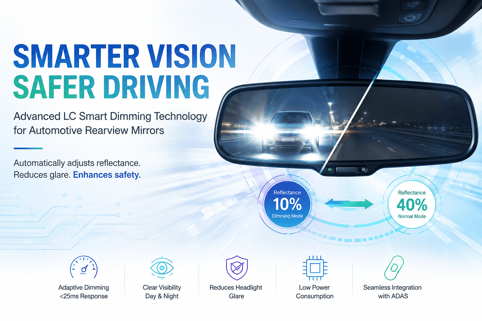
Our solution further enhances this performance by integrating Liquid Crystal (LC) smart dimming technology. Under normal driving conditions, the mirror provides clear visibility. When the system detects a potential glare hazard—such as intense headlights from a vehicle behind—it automatically switches to a dimming mode, reducing the mirror reflectance to approximately 10%. This significantly suppresses glare while maintaining sufficient rearward visibility, improving both driving comfort and safety during nighttime operation.

Regulatory Requirements

Country/Region Main Regulation / Standard Application Scope Minimum Mirror Reflectance Requirement Remarks
Europe (EU) UNECE Regulation No.46 (R46) Interior/exterior rear-view mirrors and indirect vision systems ≥40% The primary regulation in Europe; electrochromic auto-dimming mirrors are allowed to reduce reflectance at night.
United States FMVSS 111 Rear visibility mirrors Industry products commonly achieve 60–85%) Focuses more on field of view and mirror performance; unlike UNECE R46, FMVSS 111 does not define a single universal reflectance requirement for all mirrors.
Canada CMVSS 111 Rear-view mirror systems Generally follows North American FMVSS requirements Requirements are similar to those in the United States.
China GB 15084 Performance and Installation Requirements of Indirect Vision Devices for Motor Vehicles Interior and exterior rear-view mirrors ≥40% Requirements are largely aligned with UNECE R46
Japan JIS / Road Vehicle Safety Standards (aligned with UNECE regulations) Rear-view mirrors ≥40% Requirements are largely aligned with UNECE R46
South Korea KMVSS (Korean Motor Vehicle Safety Standards) Rear-view mirrors ≥40% Requirements are largely aligned with UNECE R46
Australia ADR 14 Rear vision mirrors ≥40% Requirements are aligned with UNECE R46.
Mexico NOM-related regulations Rear-view mirrors Approximately ≥40% Requirements are generally close to the North American market.


Most global automotive rearview mirror regulations are harmonized around a minimum reflectance requirement of approximately 40%, with UNECE R46 serving as the primary reference standard. In practical mass-production applications, conventional glass mirrors typically achieve 70–85% reflectance, while advanced technologies such as electrochromic (EC) mirrors, LC digital mirrors, and smart rear-view mirror systems require additional consideration of optical performance, glare reduction, and night-time visibility.


Smart Dimming: The Future of Automotive Rearview Mirrors

As the automotive industry moves toward digital cockpits, intelligent sensing, and software-defined vehicles, rearview mirrors are evolving from passive reflective components into smart optical systems.

Compared with conventional fixed-reflectance mirrors, Liquid Crystal (LC) smart dimming technology offers several advantages:

  • Fast response (<25ms) to changing lighting conditions
  • Continuously adjustable reflectance for optimal driver comfort
  • Reduced headlight glare during nighttime driving
  • High optical clarity under daytime conditions
  • Low power consumption and long service life
  • Easy integration with ambient light sensors, cameras, and ADAS systems

By dynamically controlling mirror reflectance instead of relying on a fixed optical design, LC technology provides an optimal balance between visibility, safety, and driver comfort under all driving conditions.

Smart LC mirror with dimming function (right)


Conclusion

Mirror reflectance is one of the key optical parameters affecting driving safety. While international regulations generally require a minimum reflectance of approximately 40%, modern intelligent vehicles demand more than regulatory compliance—they require adaptive optical performance.

Liquid Crystal smart dimming technology enables rearview mirrors to automatically adjust reflectance according to ambient lighting conditions, significantly reducing glare without sacrificing image quality. As automotive displays and smart cockpit technologies continue to evolve, LC-based smart mirrors are expected to play an increasingly important role in enhancing both safety and the overall driving experience.


Looking for an advanced LC smart dimming solution for your automotive mirror application? Contact us to learn how our automotive-grade LC technology can help improve optical performance, driver safety, and user experience.

If you have any questions, please contact our engineering.

author-avatar

About Alex Wang

Orient Display - Technical Engineer

Displays

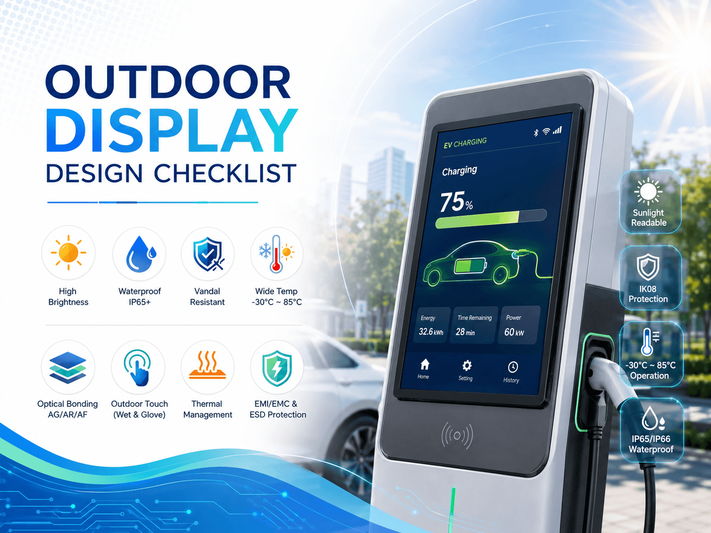
Outdoor Display Design Checklist

  1. Display Module Body

  • IPS LCD: Wide viewing angles, suitable for outdoor multi-user and multi-angle viewing .
  • LTPS LCD: An option if feasible and budget permits; offers a high aperture ratio to lower power consumption.
  • High-Brightness Backlight: Generally 1000–1500 nits is recommended; consider 1500–2500 nits for intense direct sunlight environments .
  • Wide-Temperature Liquid Crystal Materials: Recommended operating temperature of at least -30°C to +85°C to avoid slow response times at low temperatures and blackouts at high temperatures .
  • High Contrast / High Color Gamut: Under outdoor sunlight, readability is much more critical than mere brightness .
  • Anti-UV Aging Design: Outdoor UV stability must be considered for the polarizer, OCA, and cover glass printing ink .
  • Wide Viewing Angle & Polarized Sunglasses Compatibility: When using IPS, verify whether the polarizer supports a Quarter-Wave Plate (1/4 wave plate). Otherwise, the screen will turn black at certain angles when users wear polarized sunglasses .In this case, sunglasses friendly film should be used.
  • Heating Module (Heater): In extremely cold regions (e.g., -30°C), liquid crystals slow down or stop working entirely . An ITO heating glass or low-power heating wire must be designed into the rear side to preheat the screen before boot-up.
  1. Optical Bonding & Surface Treatment

  • OCA / OCR Full Bonding: Eliminates the air layer to reduce reflections, improving sunlight readability while enhancing structural strength .
  • AG (Anti-Glare) Treatment: Reduces reflections from sunlight and vehicle headlights .
  • AR (Anti-Reflection) Coating: Lowers surface reflectivity to increase contrast.
  • AF (Anti-Fingerprint) Coating: Highly recommended for touchscreens to minimize oil and water stains. Outdoor surfaces accumulate dust and fingerprint oils easily. The surface treatment is typically a 3-in-1 AG + AR + AF combination .
  • AR/AG Film: Used if the surface hardness requirement allows for below 3H.
  • IR (Infrared) Reflective Film / Heat Insulation Film: Reduces solar infrared heat entering the LCD, mitigating the risk of high-temperature blackouts .
  • UV Cut Film: Protects the liquid crystals, polarizer, and OCA bonding materials .
  1. Cover Glass & Structural Strength

  • Vandal-Resistant & Thick Cover Glass: Outdoor equipment is vulnerable to vandalism . The cover must use high-strength tempered glass (such as Corning Gorilla Glass or Asahi Glass/AGC) with a typical thickness of 4mm – 6mm to meet IK07–IK10 impact protection ratings .
  • Edge Silk-Screen Shading: Prevents backlight bleeding and protects bonding materials from light exposure.
  • Anti-Shatter Film / Safety Film: Worth considering for public spaces to prevent glass shards from scattering if broken.
  • Waterproof Structure: The target is usually IP65 / IP66 . Focus areas include the glass-to-housing interfaces, connectors, and drainage paths .
  1. Backlight & Thermal Management

  • Aluminum Alloy Backplate Heat Dissipation: High-brightness LEDs generate massive heat and require an efficient thermal conduction path .
  • Thermal Pads / Thermal Interface Materials (TIM) / Graphene: Connects the LED PCB, aluminum backplate, and the primary enclosure .
  • Local Dimming (Mini-LED) or Brightness Throttling Strategy: Automatically dims the screen at high temperatures to protect the LEDs and LCD from thermal damage .
  • High-Efficiency Backlight Driver: To reduce heat generation, the conversion efficiency of the backlight constant-current driver must exceed 90% .
  • Temperature Sensors: Recommended placement near the LED light strips, LCD backplate, and main driver board .
  • Direct Sunlight Thermal Design: Consider not only the ambient temperature but also the internal temperature rise caused by solar radiation .
  1. Touch Design

  • Outdoor Waterproof Touch (Wet Touch): Raindrops will settle on the screen surface . The touch IC (e.g., Microchip, Cypress, EETI, etc.) must support thick cover glass + operation with water + gloved operation.
  • Thick Cover Glass Touch Tuning: If the glass layer is thick, verify that the IC driver capability is strong enough.
  • Fully Sealed Design (IP Rating): Waterproof design between the front touch module and the housing structure requires high-elasticity waterproof foam (like PORON or waterproof resin) . The front surface generally needs to achieve IP65 or IP66 .
  • EMI/EMC Protection: The interior of a charging pile contains high voltage and large currents, producing intense high-frequency switching noise . Display signal lines (LVDS/eDP) and driver boards must feature robust electromagnetic shielding to prevent screen flickering or touch failure .
  • Grounding & Shielding: Ensure proper grounding for the touch FPC, cover glass ITO, and metal frame .
  1. Environmental Reliability

  • High and Low-Temperature Operation / Storage
  • Thermal Shock
  • High Temperature & High Humidity
  • UV Aging
  • Salt Spray Testing: Required if deployed near coastal areas or long-term outdoor exposure .
  • Condensation Protection
  • Resistance to Rain, Dust, and Cleaning Agents
  • Risk assessment for polarizer yellowing, OCA yellowing, and bubbling under prolonged sun exposure .
  1. Electrical & Interfaces

  • Power margin headroom for the high-brightness backlight driver
  • LED constant-current driver protection
  • Over-temperature protection
  • ESD (Electrostatic Discharge) protection
  • EMI/EMC design
  • Interface Selection: LVDS, MIPI, eDP, or HDMI, depending on screen size and the main controller platform.
  • Long-Cable Transmission Stability: Pay close attention to signal integrity if the internal wiring harnesses are long .
  1. Readability & System Strategies

  • Ambient Light Sensor (ALS): For automatic brightness adjustment .
  • Nighttime Low-Brightness Mode: Avoids blinding users and reduces power consumption .
  • Smart Dimming (Auto-Dimming): Built-in photosensitive sensor . Runs at ultra-high brightness during the day to combat glare and drops to low brightness (e.g., 100 nits) at night for anti-glare and energy saving .
  • Anti-Burn-In / Anti-Image Sticking Strategy: Although LCDs do not behave like OLEDs, displaying static UI elements for a long time can still cause image sticking .
  • High-Contrast UI Design: Using overly thin or light-colored fonts is not recommended for outdoor screens .
  1. Recommended Key Combination

For an outdoor high-brightness display on a charging pile, the following configuration is highly recommended:

IPS LCD + 1000–2000 nits High-Brightness Backlight + Full OCA/OCR Bonding + AG/AR/AF Cover Glass + IR/UV Cut Film + Aluminum Alloy Heat Dissipation Backplate + PCAP Outdoor Touch + Over IP65/IK08 Structural Design + ALS Auto-Dimming + High-Temperature Throttling Protection.


If you have any questions, please contact our engineering.

Displays

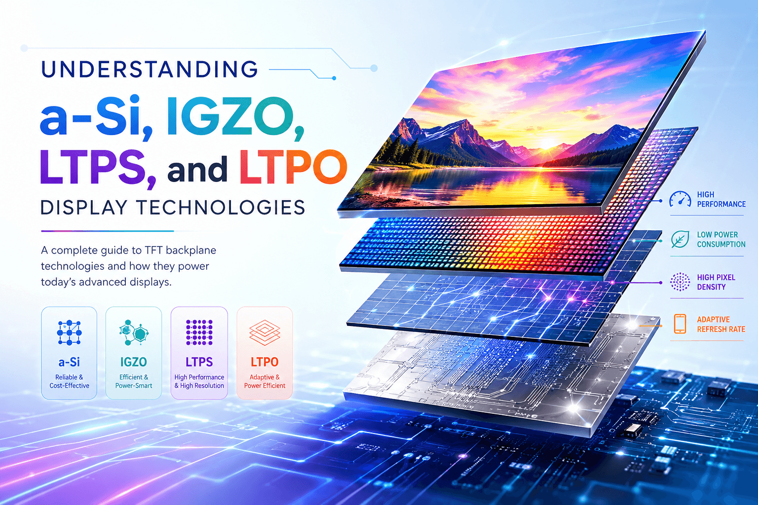
Understanding a-Si, IGZO, LTPS, and LTPO Display Technologies

As display technology continues to evolve, consumers are increasingly seeing terms like a-Si, IGZO, LTPS, and LTPO in product specifications. While these names are often associated with LCD or OLED displays, they do not describe the display panel itself. Instead, they refer to the thin-film transistor (TFT) backplane technology that controls every individual pixel.

The TFT backplane plays a critical role in determining display performance, including resolution, refresh rate, power consumption, brightness stability, and manufacturing cost.

This article explains how these four technologies work, compares their strengths and weaknesses, and discusses where each is best suited.


1. The Role of the TFT Backplane

A simplified display structure consists of:

  • Backlight (for LCD)
  • TFT Backplane
  • Liquid Crystal Layer (LCD only)
  • Color Filter
  • Polarizers

For OLED displays, the backlight is eliminated, but the TFT backplane remains essential because each OLED pixel must be individually driven.

The TFT backplane acts like millions of tiny switches that control each pixel. Different TFT technologies determine how efficiently and accurately those pixels can be driven.


2. Evolution of TFT Technologies

The development of TFT technologies generally follows this path:

a-Si

├────────► IGZO

└────────► LTPS

LTPO

Each new generation improves performance while introducing additional manufacturing complexity and cost.


3. a-Si (Amorphous Silicon)

Overview

Amorphous Silicon (a-Si) is the oldest and most widely adopted TFT technology. It has been the industry standard for LCD manufacturing for more than two decades.

Unlike crystalline silicon, amorphous silicon has a disordered atomic structure. As electrons move through the material, they encounter many obstacles, resulting in relatively poor electrical performance.

Typical electron mobility:

0.5–1 cm²/V·s


Advantages

Lowest Manufacturing Cost

a-Si benefits from mature manufacturing processes, high production yields, and relatively inexpensive equipment.

It remains the preferred choice for:

  • Large LCD televisions
  • Office monitors
  • Entry-level notebooks
  • Budget smartphones


Excellent Manufacturing Yield

Because the fabrication process is simple and well established, manufacturers can achieve consistently high yields, making a-Si highly cost-effective.


Ideal for Large Panels

Large displays such as:

  • 65-inch TVs
  • 75-inch TVs
  • 85-inch TVs
  • 98-inch TVs

are still predominantly manufactured using a-Si TFT technology.


Limitations

a) Low Electron Mobility

The relatively slow movement of electrons limits charging speed for each pixel.

As a result, a-Si struggles with:

  • Ultra-high resolutions
  • Very high pixel densities
  • Extremely high refresh rates

For example:

  • 4K at 60 Hz is well within its capability.
  • 4K at 240 Hz becomes extremely difficult.


b) Higher Power Consumption

Because leakage current is relatively high, pixels require more frequent refreshing, increasing overall power consumption.


c) Not Suitable for OLED

OLED pixels require stable current control rather than simple switching. The electrical characteristics of a-Si make it unsuitable for driving OLED panels.


IGZO (Indium Gallium Zinc Oxide)

Overview

IGZO is an oxide semiconductor technology that offers significantly higher electron mobility than a-Si while maintaining extremely low leakage current.

Typical electron mobility:

10–50 cm²/V·s

This represents roughly a 10–50× improvement over a-Si.


Advantages

Excellent Power Efficiency

One of IGZO’s greatest strengths is its extremely low leakage current.

Pixels can maintain their electrical charge for much longer, reducing the need for constant refreshing.

This makes IGZO particularly efficient when displaying static content such as:

  • Documents
  • Web pages
  • PDFs
  • Spreadsheets


Higher Resolution Support

The improved mobility allows significantly higher pixel density, making IGZO well suited for Retina-class displays.


High Refresh Rate Capability

IGZO comfortably supports:

  • 120 Hz
  • 144 Hz
  • 165 Hz

making it an excellent choice for premium LCD products.


Perfect Match for Mini LED LCD

Mini LED displays rely on thousands of local dimming zones that require fast and precise control.

IGZO provides the speed and efficiency needed for these premium displays.


Limitations

  • Higher Manufacturing Cost

Compared to a-Si, IGZO requires more advanced materials and manufacturing equipment.


  • Lower Mobility than LTPS

Although much faster than a-Si, IGZO still cannot match the extremely high electron mobility of LTPS.

For applications demanding maximum pixel density and the fastest switching speeds, LTPS remains superior.


LTPS (Low Temperature Polycrystalline Silicon)

Overview

LTPS is created by transforming amorphous silicon into polycrystalline silicon using laser annealing.

The resulting crystal structure allows electrons to move much more freely.

Typical electron mobility:

100–200 cm²/V·s

This is over 100 times faster than a-Si.


Advantages

Extremely High Pixel Density

LTPS can support pixel densities exceeding:

  • 500 PPI
  • 600 PPI
  • 700 PPI

making it ideal for smartphones and other compact displays.


Excellent High Refresh Rate Performance

LTPS easily supports:

  • 120 Hz
  • 165 Hz
  • 240 Hz

and even higher refresh rates.


Smaller TFTs

Because LTPS transistors are more efficient, they occupy less space.

This allows:

  • Narrower bezels
  • Higher aperture ratio
  • Improved display efficiency


Ideal for OLED

OLED displays require precise analog current control for every pixel.

LTPS provides the high drive capability necessary for excellent OLED image quality.

Today, most smartphone OLED displays use LTPS technology.


Limitations

Higher Leakage Current

The same characteristics that enable high-speed operation also increase leakage current.

Static images therefore consume more power compared with IGZO.


More Expensive Manufacturing

Laser annealing equipment is expensive, and process control is considerably more complex than for a-Si or IGZO.


LTPO (Low Temperature Polycrystalline Oxide)

Overview

LTPO is not a completely new semiconductor material.

Instead, it combines the strengths of both LTPS and IGZO within the same TFT backplane.

A simplified view is:

  • LTPS provides high-speed pixel driving.
  • IGZO minimizes leakage current and maintains pixel charge.

Together, they deliver both high performance and excellent energy efficiency.


The Biggest Advantage of LTPO: Variable Refresh Rate

The defining feature of LTPO is its ability to dynamically adjust refresh rate over a very wide range.

For example:

  • 1 Hz while displaying a static image
  • 10 Hz during Always-On Display mode
  • 30–60 Hz for reading
  • 90–120 Hz while scrolling
  • 120–165 Hz during gaming

This dramatically reduces power consumption without sacrificing responsiveness.


Always-On Display

LTPO enables displays to refresh at just 1 Hz, allowing the screen to remain active while consuming minimal power.

This capability has become a defining feature of flagship smartphones and smartwatches.


Technology Comparison

Feature a-Si IGZO LTPS LTPO
Electron Mobility Low Medium Very High Very High
Power Consumption Medium Very Low Medium Very Low
Leakage Current High Extremely Low High Low
High PPI Support Fair Good Excellent Excellent
High Refresh Rate Fair Good Excellent Excellent
Variable Refresh Rate Limited Limited Limited Outstanding
OLED Compatibility Poor Limited Excellent Excellent
Manufacturing Cost Lowest Medium High Highest
Manufacturing Complexity Low Medium High Very High


Typical Applications

a-Si

  • LCD televisions
  • Office monitors
  • Budget laptops
  • Industrial displays

IGZO

  • Premium LCD monitors
  • Mini LED displays
  • Tablets
  • Professional monitors

LTPS

  • Smartphone OLED displays
  • High-resolution mobile LCDs
  • AR/VR displays

LTPO

  • Flagship smartphones
  • Smartwatches
  • Premium OLED mobile devices


Which Technology Is Best?

There is no single “best” TFT technology. Each one is optimized for different priorities.

  • a-Si remains the most economical solution for large displays where cost is the primary concern.
  • IGZO provides an excellent balance of power efficiency, image quality, and performance, making it ideal for premium LCD products.
  • LTPS delivers the highest driving capability and pixel density, making it the preferred choice for smartphone OLED displays.
  • LTPO combines the speed of LTPS with the efficiency of IGZO, enabling adaptive refresh rates and significantly improved battery life. It has become the technology of choice for today’s flagship mobile devices.


Final Thoughts

Although consumers often focus on display resolution or brightness, the TFT backplane technology is one of the most important factors determining the overall user experience.

From the affordability of a-Si, to the efficiency of IGZO, the high performance of LTPS, and the adaptive intelligence of LTPO, each technology represents a different balance between cost, power consumption, and display capability.

Understanding these technologies helps explain why different products—from budget monitors to premium smartphones—are built the way they are, and why manufacturers continue to invest in more advanced TFT backplane technologies as display performance continues to evolve.

If you have questions or would like to explore your next design, please contact our engineering.

Displays

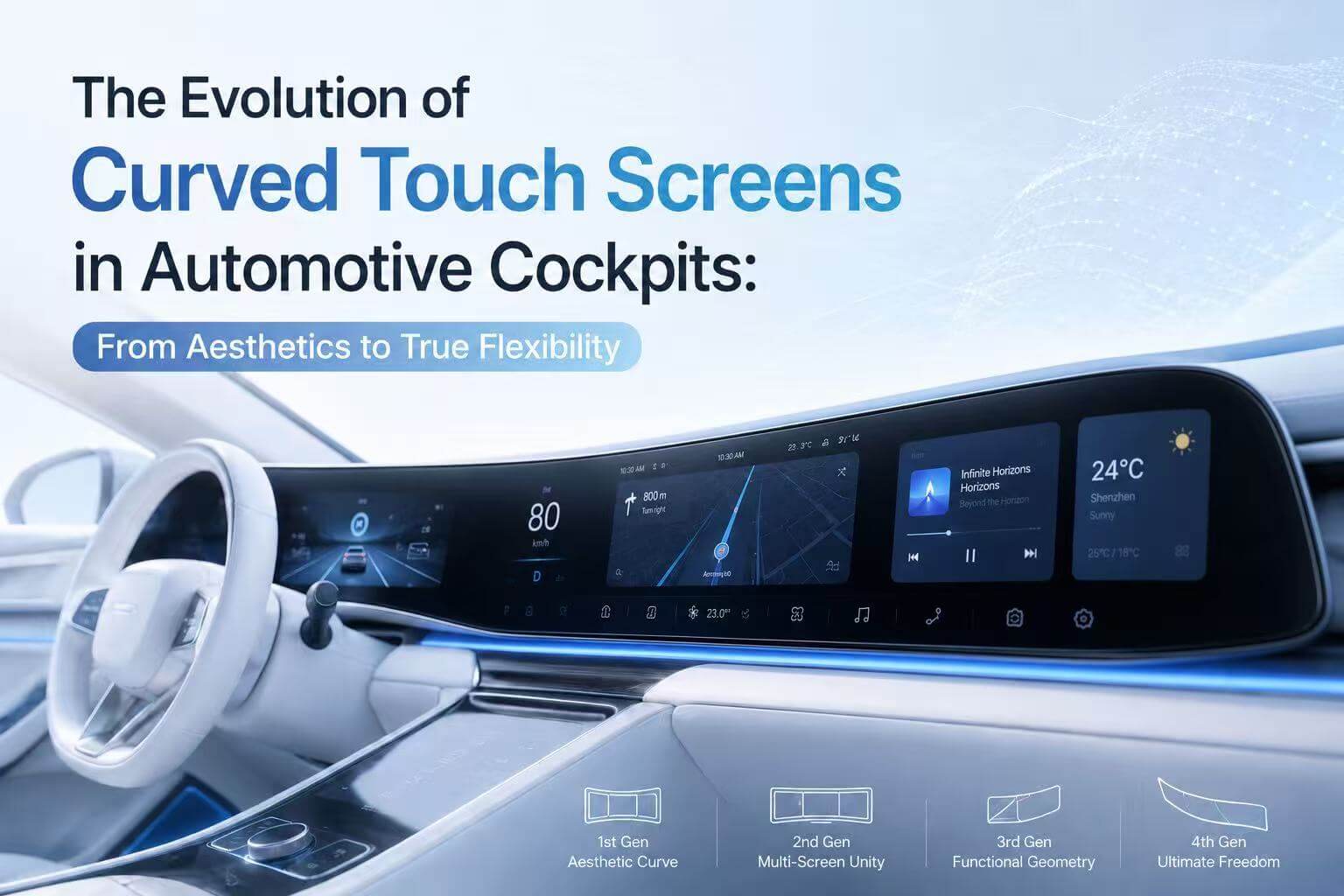
The Evolution of Curved Touch Screens in Automotive Cockpits: From Aesthetics to True Flexibility

The modern automotive cockpit is undergoing a massive design shift. Gone are the days of rigid, flat, rectangular screens slapped onto the center console. Today, tiers and OEMs are treating the dashboard as a continuous, flowing canvas.

Designing a Curved Touch Screen introduces unique optical, mechanical, and manufacturing complexities that don’t exist with flat glass. Understanding how these screens are built—and where the technology is heading—is crucial for display engineers, product managers, and industrial designers alike.

Let’s break down the four distinct generations of curved touch screen technology, evaluating the mechanical engineering, bonding constraints, and material science behind each.


The 4 Generations of Curved Touch Screen Technology

1st Gen: The “Aesthetic” Curve (IML + Flat Glass Touch)


In the early days of curved automotive interiors, the display technology wasn’t curved. The active display area and button area remained completely flat.

Instead, the curvature was restricted entirely to the border/mid area using In-Mold Labeling (IML) or injection-molded plastic trim. A flat glass touch panel was embedded inside a curved housing. While this achieved a fluid look on the dashboard, it lacked seamless integration; the distinct boundary between the flat screen and the curved plastic frame remained highly visible.


2nd Gen: The Multi-Screen Unity (Cold Bending Lens + Glass Touch)

To achieve a premium, single piece look without a massive price tag, the industry developed Cold Bending. This is currently the dominant technology for large, integrated dual or triple-screen setups (the “pillar-to-pillar” display).

  • The Architecture: The underlying LCD display panels and touch sensors are flat, but they are covered by a single, large sheet of protective glass that is curved in the middle or at the borders.
  • The Process: Glass is chemically strengthened while perfectly flat. During final assembly, it is mechanically forced into a curved bezel frame at room temperature.
  • Engineering Advantage: Because the glass isn’t heated, it retains pristine optical quality, suffers no thermal distortion, and keeps manufacturing costs relatively low. However, it is strictly limited to shallow, gentle 2D cylindrical bends because the glass remains under constant internal mechanical stress.


3rd Gen: Functional Geometry (Hot Bending Lens + Glass/Film Touch)

When a design demands aggressive curves,  or a complex 3D shape—cold bending fails, which is Hot Bending.

  • The Architecture: The primary display area remains flat (to accommodate rigid LCDs), but the button/control area transitions into a steep curve, forming a waterfall screen or an L-shaped console.
  • The Process: Flat glass is placed over a precise graphite mold and heated to its softening point (around 600°C–700°C). Gravity or pressure shapes the glass to the mold. Crucially, chemical strengthening must happen after this thermal process, otherwise, the heat destroys the tempering layer.
  • The Challenge: Because the touch area now wraps around a tight radius, traditional rigid Glass-on-Glass (GG) touch sensors can crack. Engineers must transition to Film-based touch sensors (Metal Mesh or AgNW on PET) that can flex to conform to the inner curvature of the hot-bent lens.


4th Gen: Ultimate Freedom (True Flexible Touch & Display)

The cutting edge of cockpit design abandons flat internal components altogether. In the 4th generation, both the display area and the touch sensor are natively curved.

  • The Architecture: The screen seamlessly flows along the contours of the dashboard, fitting curved instrument clusters or wrapping around the driver in a semi-enclosed cockpit.
  • The Technology: This relies on Flexible OLED substrates paired with CPI (Colorless Polyimide) or ultra-thin flexible touch sensors.
  • Performance Metrics: These assemblies utilize sensors engineered to withstand tight bending radius,  and endure over 200,000 bending cycles, offering massive design freedom while maintaining high reliability in harsh environments (operating from -40C up to 95C).


Key Engineering Challenges in Curved Display Design

Whether implementing a Gen 2 cold-bent system or a Gen 3 hot-bent module, front-end design requires balancing several physical trade-offs:

  1. Bonding Methodology: OCA vs. OCR

Connecting a curved cover lens to the display panel is a major yield-rate variable.

  • OCA (Optically Clear Adhesive) Tape: Standard flat OCA films tend to struggle on curved surfaces. The internal rebound stress of the bent glass causes the tape to pull away at the edges, leading to delamination and bubbles over time.
  • OCR/LOCA (Optically Clear Resin / Liquid Glue): Liquid bonding is highly preferred for curved geometries. The liquid flows naturally to fill the uneven tolerances and gaps created by the curve. However, it requires highly specialized fixture tooling to prevent overflow and ensure a completely uniform bond-line thickness across the bend.
  1. Optical Distortion and Reflection Management

Curved surfaces inherently behave like lenses. As the radius of curvature sharpens, light traveling from the flat display through the curved glass bends, causing visual distortion, ghosting, or color shifts at wide viewing angles.

Furthermore, while flat glass reflects ambient light in one predictable direction, a curved surface captures and concentrates glare from multiple angles. Specifying high-performance Anti-Reflective (AR) and Anti-Glare (AG) coatings is mandatory. However, depositing these coatings uniformly across a steep 3D curved surface without pooling or thinning at the apex is a major manufacturing hurdle.

  1. Dimensional Tolerance Stack-up

Thermal bending introduces minor batch-to-batch variations in the exact radius of curvature. If the inner radius of your cover glass doesn’t perfectly match the profile of the display or mounting bracket, it creates uneven pressure points. In production, this can cause localized pooling of liquid glue, leading to visual artifacts on the display (the Mura effect) or, worse, causing the display panel to crack under mechanical stress.


Conclusion

The evolution of the curved touch screen is a journey of removing mechanical constraints from user experience design. While Gen 2 cold bending offers an excellent middle ground for cost-effective, wide screen setups today, the future belongs to Gen 4 flexible architectures.

As material science advances in flexible substrates and high-reliability liquid optical bonding, the dashboard will transition from a place where displays are mounted, to a surface that is entirely a display.

If you have questions or would like to explore your next design, please contact our engineering.

author-avatar

About Lily Liang

Orient Display - Account Manager

Displays

SPI Displays Are Not Video Streams: Understanding Command Mode LCDs

SPI Command Mode LCDs: The Day I Realized Most “SPI Displays” Aren’t Really Streaming Video

When I first started working with embedded displays, I always believed I was using a “pure SPI display.” The MCU continuously sent data through SPI, the screen updated in real time, and from the outside it looked exactly like video streaming. But after digging deeper into how LCD controllers actually work, I realized something important:

Most so-called “SPI displays” are not true streaming displays at all. They are actually Command Mode Displays with internal memory.

And honestly, that realization completely changed how I think about embedded display systems.


What Is an SPI Command Mode Display?

An SPI Command Mode LCD is a display where the MCU sends commands and image data through SPI, while the display controller itself handles the actual screen refreshing.

The key reason is simple:

The display driver IC contains internal frame memory, usually called GRAM (Graphics RAM). Once image data is written into GRAM, the display controller continuously refreshes the panel automatically. The MCU only updates the content when something changes.

In other words:

  • MCU updates the image
  • The display handles the refreshing

The MCU does not continuously “feed” the display.


Why These Displays Are So Popular

SPI command displays are extremely common in embedded systems because they simplify both hardware and software design. They offer several major advantages:

Lower Pin Count

SPI interfaces typically require only a few signals:

  • MOSI
  • MISO
  • SCK
  • CS
  • DC

Compared to RGB interfaces, routing is much simpler and connectors can be much smaller.

Lower EMI

SPI uses serial communication with relatively low bandwidth compared to parallel video interfaces. That usually means:

  • Lower EMI
  • Easier EMC design
  • Better suitability for industrial and medical products

Partial Refresh Support

This is one of the biggest advantages. Instead of refreshing the entire screen, the MCU can update only the region that changes.

For example:

  • Updating the whole screen may require over 100 KB of data
  • Updating only several digits may require just a few KB

That significantly reduces bandwidth and power consumption.


Real-World Embedded Products

Many modern embedded display modules are built around command-mode display architectures with internal GRAM.

For example, our P Series SPI display modules use SPI command interfaces together with onboard display controllers, making them suitable for industrial HMIs, medical devices, handheld devices, and other embedded systems where low EMI and partial refresh are important.

Some products simplify the architecture even further. Our AGN/AGU UART display modules allow the host MCU to communicate through high-level UART commands, while the display module internally handles rendering, framebuffer management, and screen refreshing. This significantly reduces MCU workload and simplifies embedded software development.

We also provide ACN series MCU-interface display modules, which are designed for embedded systems requiring direct MCU communication together with command-based display control architectures.

In many cases, developers are not directly driving LCD pixels at all. They are simply updating display content while the display controller manages the actual refresh process internally.


Why SPI Feels Like Video Streaming

This misunderstanding is actually very common. I had it myself for years. And honestly, it makes perfect sense.


  1. SPI Looks Continuous

SPI can transfer data very quickly.

In many projects, we continuously send image data through SPI, sometimes even refreshing the full screen repeatedly.

Visually, it feels exactly like streaming video.


  1. The Name “SPI Display” Is Misleading

People constantly say things like:

  • SPI LCD
  • SPI display
  • SPI screen

The focus is always on the communication interface, not the display architecture itself. So naturally, many engineers unconsciously assume: SPI = directly driving pixels in real time; But actually: SPI is only the transport method.

The display mode is a completely separate concept.


  1. Driver Libraries Hide the Commands

In application code, we often write something simple like:

LCD_DrawImage(…);

But underneath that function, the driver is actually:

  • Setting display windows
  • Configuring GRAM addresses
  • Sending commands
  • Starting memory writes

All of this is heavily abstracted away.

So over time, it feels like:

“I’m just continuously sending image data.”

Even though the display is actually operating in command mode the entire time.


  1. We Are Updating Memory, Not Driving Pixels

This was the biggest mental shift for me.

Most SPI displays internally store image data inside GRAM.

What we are really doing is:

Writing image data into the display’s internal framebuffer. The display controller then takes care of refreshing the panel itself. That is fundamentally different from true video streaming.

And because this process is mostly invisible to developers:

  • We never see the refresh timing
  • We do not manage line scanning
  • The image remains even after SPI stops

It creates the illusion that we are directly driving the panel. But we are not. We are simply updating what the display should show.


Command Mode vs Video Mode

The core difference is actually very simple.

Command Mode Video Mode
Internal GRAM exists Little or no framebuffer
Display refreshes automatically Continuous pixel stream required
MCU updates when needed MCU continuously outputs frames
Partial refresh supported Usually full-frame streaming
Image remains after communication stops Display stops without input

Typical command-mode interfaces:

  • SPI
  • MCU/8080 interfaces

Typical video-mode interfaces:

  • RGB Parallel
  • LVDS
  • MIPI DSI Video Mode


The Most Important Realization

Eventually I realized something very important:

I was never truly driving pixels in real time.
I was only updating what the display should show.

The display itself was handling the refreshing all along.

And once I understood that:

  • Bandwidth calculations made more sense
  • Partial refresh became intuitive
  • EMI behavior became easier to understand
  • MCU optimization became much clearer

Many embedded display design decisions suddenly stopped feeling mysterious.


Final Thoughts

Looking back, this misunderstanding is incredibly common because several factors combine together:

  • SPI visually resembles streaming
  • Full-screen refreshes imitate video behavior
  • Driver libraries hide the commands
  • Internal GRAM is invisible to developers
  • “SPI display” terminology is misleading

So, it becomes very natural to assume:

“SPI displays are continuously streamed displays.” But in reality, most of them are better understood as: A display terminal with built-in memory.

And honestly, once you realize that difference, you start thinking about embedded displays in a completely different way.


If you have questions or would like to explore your next design, please contact our engineering.

author-avatar

About Veronica Chen

Orient Display - Technical Support

Displays

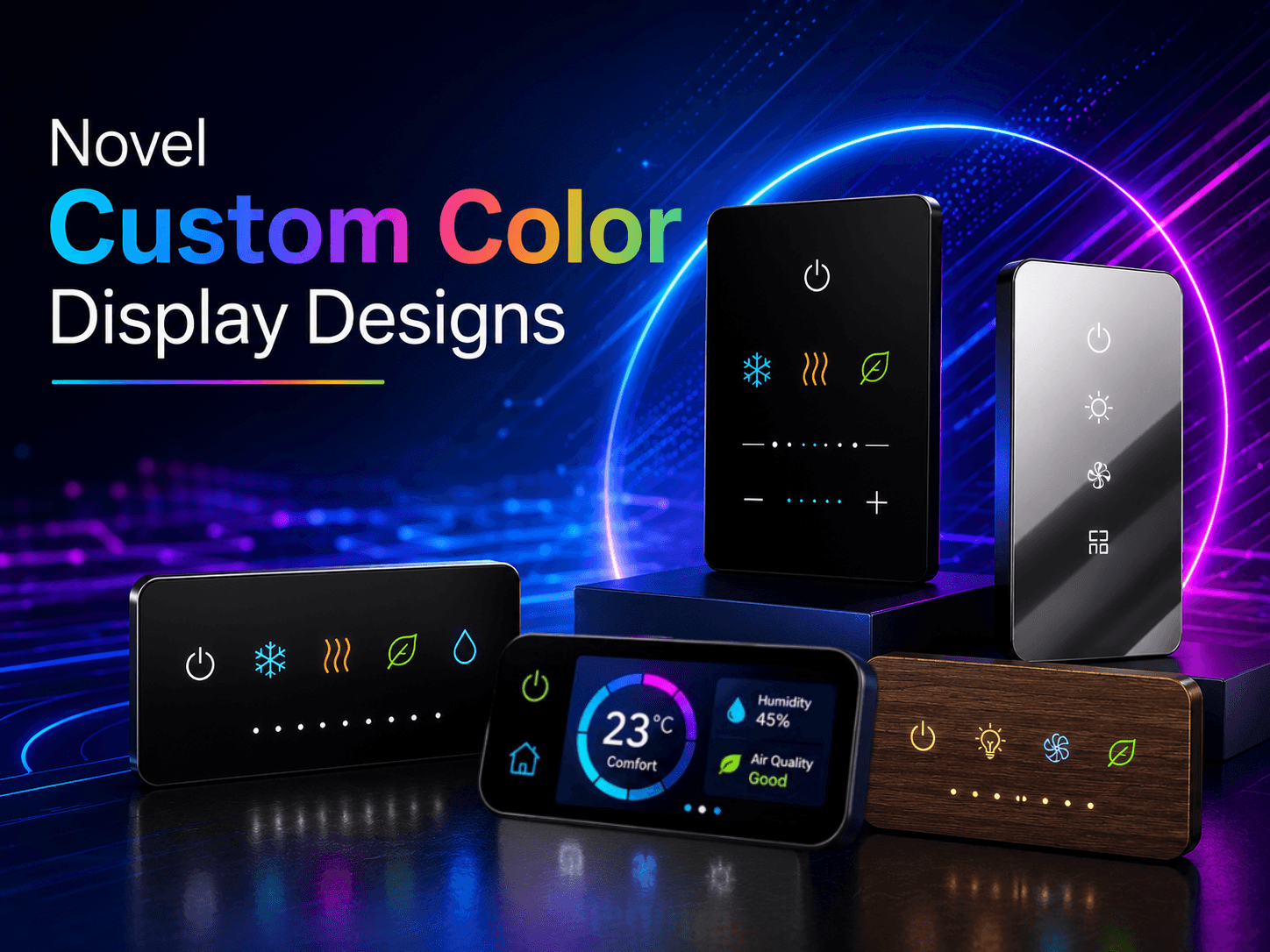
Novel Custom Color Display Designs

Designers often envision color displays that can be created in any shape or size to perfectly match their product aesthetics. In reality, however, display designs are typically constrained by standard TFT or OLED panel sizes.

Customizing a TFT or OLED display can be prohibitively expensive due to high non-recurring engineering (NRE) costs. For example, developing a custom display at Gen 5 TFT production line can require an investment of approximately $300,000 to $400,000. In addition, development cycles are long and generally only feasible for high-volume projects.

To address these challenges, the engineering team at Orient Display has explored innovative approaches to enable more flexible and visually appealing display designs. These concepts have proven highly useful for designers seeking customization without the cost of fully custom panels. Most of these solutions are based on dead-front (all-black) display designs, which offer both aesthetic and functional advantages.


What is a Dead-Front Display?

A dead-front display is a user interface panel that appears completely uniform, such as black, matte black, white, silver, mirror-like, or even wood-textured. When turned off. In this state, all icons, text, and graphics are fully hidden, creating a seamless and minimalist surface.

When the display is illuminated by a backlight, the hidden elements become visible. This creates a clean, high-end, and modern visual effect, making dead-front displays especially popular in applications such as automotive dashboards, smart home appliances, and control panels.

From left to right: Black Dead Front Display, White Silver Dead Front Display, Mirror Dead Front Display


Wood Texture Dead Front Display


If in-house visual assets are limited, the Google Nest design team provides excellent examples of well-integrated display aesthetics, as shown below.


We will further explore black dead-front display concepts in the following design approaches.

Design 1:  Limited Colors With Fixed-Position Color Displays

For products that require simplicity, clarity, and cost efficiency, this approach delivers elegant results.

By using screen printing to define up to three colors in fixed positions, designers can create clean, intuitive interfaces with strong visual contrast. When the display is off, the surface remains perfectly uniform; when illuminated, only the intended elements appear—crisp and refined.

Why it works:

  • Cost-effective solution for mass production
  • High reliability and stable color performance
  • Ideal for appliances, industrial controls, and minimalistic UI designs


Design 2: Unlimited or Gradient Colors with Fixed-Position Color Displays

When your product demands richer visuals or a more premium feel, this approach removes the limitations of traditional color printing.

Instead of relying on screen printing, color films laminated onto the polarizer enable vibrant, multi-color or gradient effects with superior consistency. This allows designers to create visually striking interfaces that stand out in competitive markets.

To ensure optimal visual quality, we recommend maintaining at least 2 mm spacing between color segments to prevent crosstalk.

Why it stands out:

  • Enables unlimited or gradient color designs
  • Delivers a more premium, high-end appearance
  • Ideal for smart home devices, consumer electronics, and branded UI experiences


Design 3: Hybrid Fixed-Position Color Displays with TFT or AMOLED

For the most advanced applications, hybrid designs combine the best of both worlds—static elegance and dynamic intelligence.

By integrating fixed-position color elements with TFT or AMOLED displays, designers can create interfaces that are both visually distinctive and functionally powerful.

Static icons, branding elements, or color zones remain crisp and consistent, while dynamic display areas provide rich content, animation, and interactivity.

What this unlocks:

  • Premium, futuristic product designs
  • Seamless integration of static and dynamic UI elements
  • Maximum design freedom without full custom panel costs

Structure of the Hybrid Passive LCD and Active TFT/AMOLED Display


From Concept to Reality

Great product design is no longer limited by standard display formats. With the right approach, you can achieve custom-looking designs without custom-level cost and risk.

At Orient Display, our engineering team works closely with customers to turn design concepts into manufacturable, high-performance display solutions.

Let’s build something distinctive together.

If you have questions or would like to explore your next design, please contact our engineering.

Displays

Solving ESD Failures in Modern Electronic Systems

Case Overview – Improving ESD Reliability in large size USB Display System

The exiting display system was upgraded from an older LVDS design to a new USB‑based architecture. During certification testing, the system passed the 8 kV contact discharge test but failed the 15 kV air discharge test. This caused video interruptions and system resets, preventing the product from being approved.

Our engineering team analyzed the issue and identified two main causes:

  1. The USB ground path had too much resistance during an ESD event.
  2. The USB power line did not have strong enough protection against voltage spikes.

After making targeted improvements, the system able to successfully pass the 15 kV air discharge test.

What Was Happening?

During testing, an ESD gun applies a high‑voltage static shock to the outside of the device. This simulates real‑world situations such as a user touching the screen after walking on carpet.

This shock caused the USB interface to momentarily fail, which led to:

  • Video freezing
  • Display blackouts
  • Touch panel communication loss
  • System resets

This happened because the USB interface is more sensitive to static electricity than the older LVDS design.


Root Cause Debug

  1. Grounding Was Too Weak for ESD

The USB ports used ferrite beads between the connector and ground. Ferrite beads are good for filtering noise, but they block fast, high‑energy ESD pulses. This prevented the static charge from safely going to ground.

  1. The USB Power Line Needed Better Protection

The USB 5 V line did not have a fast‑acting protection device to absorb sudden voltage spikes caused by ESD.


What We Changed

To fix the issue, we made four improvements:

✔ Direct Grounding

We removed the ferrite beads (L15 and L20) and connected the USB ground directly to the system ground.
This gives static electricity a clean, low‑resistance path to escape.

✔ Added TVS Protection

We added a high‑speed TVS diode (SP1326‑01LTG) to the USB 5 V line.
This device instantly clamps voltage spikes and protects the USB controller.

✔ Improved ESD Path

The new grounding and protection layout ensures that ESD energy is safely diverted away from sensitive components.

Figure 1


Figure 2


How the Improved Design Works

Before Fix

ESD Shock → Ferrite Bead → Blocked → USB Chip Overloaded → Video Failure

After Fix

ESD Shock → Direct Ground → TVS Clamp → USB Chip Protected → System Stable

Results

After applying these improvements:

  • The system passed 15 kV air discharge
  • No video dropouts or resets occurred
  • USB communication remained stable
  • The product is now ready for certification, BINGO!!

Conclusion

The ESD failures were caused by grounding impedance and insufficient surge protection in the USB interface. By optimizing the ground path and adding proper TVS protection, we restored the system’s reliability and ensured it meets certification requirements.

If you have any questions, please contact our engineering.

author-avatar

About Lily Liang

Account Manager - Orient Display

Displays

LCD Touchscreen Module Mura (Defect) and Solutions

What is Mura?

“Mura” is the Romanized spelling of the Japanese kanji “斑” (むら), which originally means unevenness, inconsistency, or defects. Because Japan was an early leader in the LCD industry, “Mura” has become a widely used technical term. It refers to various visible artifacts caused by non-uniform brightness in display panels (LCD/OLED).

This issue can occur in televisions, smartphones, and automotive dashboards. Brightness non-uniformity (Mura) affects the viewing experience, reduces the perceived premium quality of a product, and may even interfere with display performance or functionality.

In the context of optical bonding for displays, some manufacturers interpret Mura as light leakage. Since this defect may appear as yellow spots or yellowish lines along the edges on a white screen, many manufacturers also refer to Mura as “yellowing.”


Mura Evaluation (Identification Method)

The simplest way to identify Mura is to switch the display to black, white, or low gray-level images in a dark room. By visually inspecting the edges around the active area (AA), one may observe irregular colors such as white, yellow, or other uneven patterns.

Observing the display from different angles will reveal various types of Mura phenomena, including stripes, patches, and clustered patterns, with no consistent color or shape. If pressure is intentionally applied to the display area, the existing Mura will intensify, and even after removing the external force, the Mura will not disappear immediately.

From the working principle of liquid crystal displays, Mura is essentially unavoidable whenever stress is applied to the liquid crystal cell—it can only vary in severity.

Based on the principle of camera lens filters, Fujifilm developed ND (Neutral Density) filters. These filters come in eight levels: 1%, 2%, 3%, 4%, 5%, 6%, 8%, and 10%. In the industry, Mura is typically classified and evaluated according to these levels.


Neutral Density (ND) Filters

In ND filters, a 1% transmittance filter (ND100 or higher) is more “stringent” (i.e., has stronger light reduction capability) than an 8% transmittance filter (typically ND8 or ND12).

The lower the transmittance percentage of an ND filter, the less light it allows through, meaning it blocks more light and is therefore considered more “intense” or “stronger.”

Specific Comparison:

  • 1% transmittance (approximately ND100–ND1000 or higher):
    Belongs to strong ND filters, reducing light by more than 6–10 stops. Suitable for daytime long-exposure photography, such as capturing flowing water with a silky effect.
  • 8% transmittance (typically ND8–ND12):
    Belongs to weak ND filters, reducing light by about 3 stops. Suitable for shooting in cloudy conditions or at dusk, with relatively mild light reduction.

In summary: The lower the transmittance percentage, the higher the ND value, and the stronger the light reduction capability.


Causes of Mura

Mura can originate from materials or processes in the front-end manufacturing of the display panel (PANEL), though the specific solutions for those are not discussed here. It can also result from materials and processes used during the back-end assembly stages.

This article focuses only on Mura that occurs after optical bonding. Under the assumption that defects in the cover glass, panel, polarizer, backlight, and other materials have been ruled out, the discussion centers on Mura caused by deformation of the liquid crystal cell due to bonding-induced stress.

Typical examples include yellow spots and non-uniform display effects commonly observed after bonding.

Failure Analysis of Defective Units:  A detailed teardown analysis was conducted on defective units. Removing the housing showed no change, and removing the backlight also produced no change. However, after separating the CTP (capacitive touch panel) and TFT, the yellow spots disappeared. When the CTP was reattached and left to rest for several days, the yellow spots reappeared.

This confirms that the Mura defect in this case is related to the bonding materials or processes. In full-lamination processes—whether using OCA (optically clear adhesive) or liquid adhesive—Mura that appears after curing or after a period of rest is strongly related to adhesive selection and curing conditions.

Impact of Optical Adhesive:   First, considering the effect of optical adhesive: polymer-based adhesives tend to be relatively rigid. If the selected thickness is insufficient, their ability to absorb strain is poor. As a result, deformation stress affects the liquid crystal layer, transmitting mechanical distortion to the display. This leads to non-uniformity in the liquid crystal cell gap, causing uneven light transmittance and ultimately resulting in visible color non-uniformity—i.e., Mura.


Solutions for Mura

  • Increase adhesive thickness

    A thicker adhesive layer can absorb more deformation stress. However, this will increase material costs, potentially even doubling them. Therefore, it is not recommended to use OCA with a thickness of 175 μm or thinner.

  • Reduce cover glass thickness

    Thinning the cover glass can help reduce deformation. However, this may also decrease impact resistance and durability.

  • Use softer adhesive (lower elastic modulus)

    Selecting a softer adhesive can help better absorb stress. However, if the adhesive is too soft, it may become difficult to handle during the bonding process.

  • Use laminated (multi-layer) structural adhesive

    This type of adhesive combines the advantages of both thicker adhesive layers and improved stress absorption. It offers the best improvement effect. A schematic diagram of stress distribution after bonding can illustrate this advantage.

Single Layer OCA                                                    Sandwich OCA

  • Reduce bonding pressure appropriately

    Minimize lamination pressure where possible, opt for backlight assembly after bonding, and ensure the bonding platform is as flat as possible. This helps reduce excessive compression and potential damage to the liquid crystal cell.

  • Improve shrinkage behavior of liquid adhesives

    Select materials with lower curing shrinkage. In addition to changing adhesive materials, curing process parameters can also be optimized—for example, using low-intensity, longer-duration UV curing or gradual temperature ramp-up curing. These methods can help mitigate Mura to some extent.


If you have any questions, please contact our engineering.

Displays

FPC Capacitive Key: A Simple Way to Think About Touch

Sometimes when I look at the touch solutions we use every day, I get the feeling that a lot of designs exist simply because “that’s how it’s usually done,” not because they’re the only option.

Take touch screens, for example.

In most cases, when we say “touch,” we immediately think of a full capacitive touch panel—an entire surface that responds to input anywhere. It works, it’s intuitive, and for many applications, it’s absolutely the right choice.

But when the interaction is limited to just a few buttons, that kind of solution can feel a bit… heavy.


Not All Touch Needs Coordinates

The most common structure we deal with looks something like this:

Cover Lens + OCA + ITO Glass + FPC + Touch Controller

Its job is straightforward: detect where you touch (X-Y coordinates)

This makes perfect sense for interfaces that involve gestures, swiping, or dynamic UI, but not every interaction needs location tracking. Sometimes, all you really need is a simple “trigger.”


A Different Approach: CapSense

This is where capacitive sensing (CapSense) comes in. Instead of tracking position, it detects whether a specific area is being touched.

Typical structure:

Cover Lens + ITO Key (single layer) + FPC + CapSense IC

It’s commonly used for:

  • Buttons
  • Sliders
  • Fixed touch zones

Compared to full touch panels, it simplifies things—but it still relies on ITO.


Taking It One Step Further: Removing ITO

And then there’s an even simpler approach.

FPC Capacitive Key is based on a very straightforward idea:

Replace ITO electrodes with copper electrodes on FPC

Which brings the structure down to:

Cover Lens + FPC + CapSense IC

No ITO layer, no full touch stack. Just what’s necessary.


What It Actually Looks Like

Below is a simplified layout that helps visualize how this approach is implemented.

The display sits in the center; Capacitive keys are distributed around the edges; All key electrodes are routed through the FPC; Each key (A/B/C/D) corresponds to an independent sensing area.

What’s interesting here is that the display and touch inputs are no longer part of the same stack. They coexist—but remain structurally independent.


How It Works

There’s no mechanical action involved, and nothing visibly moves.

  1. Metal electrodes (copper or silver) are formed on the FPC
  2. A sensing IC continuously monitors capacitance
  3. A finger approaches → capacitance changes
  4. The IC detects it and outputs a signal

It feels less like “pressing a button” and more like being detected.


Structurally, It’s Very Simple

From a hardware perspective, the simplicity stands out:

  • Substrate: PET or PI (typically 0.1–0.3 mm)
  • Electrodes: flexible in shape (round, bar, custom)
  • Connection: direct FPC to mainboard
  • Surface: glass or plastic overlay

And one key difference: No need for full ITO film or ITO glass. That alone can open up room in both design and cost.


Manufacturing Is Fairly Straightforward

Typical approaches include:

  • Etching copper electrodes directly on FPC
  • Printing conductive paste (silver or copper)
  • Laminating a protective cover (glass or plastic)
  • Connecting via standard FPC connectors

It feels closer to circuit design than display module integration.


What Stands Out in Practice

After working with this approach, a few characteristics become quite noticeable:

  • No mechanical wear, No pressing action means longer lifespan
  • Flexible form factor, FPC allows bending and tighter layouts
  • Easier sealing, Better suited for waterproof or dustproof designs
  • Simpler structure, Works well as a standalone input module


Where It Has Limits

Of course, it’s not meant to replace everything. Some practical constraints:

  • Sensitive to environment (moisture, gloves, ESD) → requires tuning
  • Larger button areas may reduce responsiveness
  • Requires a dedicated capacitive sensing IC
  • Not transparent

That last point is easy to overlook:

Since there’s no ITO, it doesn’t support transparent or semi-transparent designs


A Simple Way to Think About It

If you strip it down to function:

  • Full interaction interface → use a touch panel
  • Fixed input zones → capacitive keys
  • Prefer a simpler structure → FPC Capacitive Key is worth considering

In the end, it’s not about choosing the most advanced solution. It’s about choosing something that fits—just enough, not more.

And sometimes, making things lighter is already an improvement.


If you have any questions, please contact our engineering.

author-avatar

About Veronica Chen

Orient Display - Technical Support