
Blog
Automotive Rearview Mirror Reflectance Requirements: Why Reflectance Matters and How It Is Controlled
Automotive rearview mirrors play a critical role in driving safety by providing drivers with clear visibility of surrounding traffic. One of the most important optical parameters of a rearview mirror is reflectance—the percentage of incident light that is reflected by the mirror surface.
A mirror with insufficient reflectance produces a dim image, while excessive reflectance may contribute to glare. Therefore, automotive mirrors are designed to meet strict optical and regulatory requirements.
What Is Mirror Reflectance?
Reflectance is the ratio of reflected light to incident light, usually expressed as a percentage. For example:80% reflectance means that 80% of the incoming light is reflected and 20% of the light is absorbed or transmitted through the mirror.
Higher reflectance generally provides Brighter images with better contrast, results improved object recognition. However, under nighttime conditions, very high reflectance can increase glare from following vehicles. If the mirror reflectance is too low, the reflected image becomes dim and lacks sufficient clarity, reducing the driver’s ability to accurately perceive objects behind the vehicle. Conversely, if the reflectance is too high, the glare from following vehicles’ headlights can become a significant distraction during nighttime driving, negatively affecting driver visibility and comfort.
For this reason, the reflectance of conventional automotive rear-view mirrors is typically designed to be around 40%, providing a balanced compromise between image brightness and glare reduction.
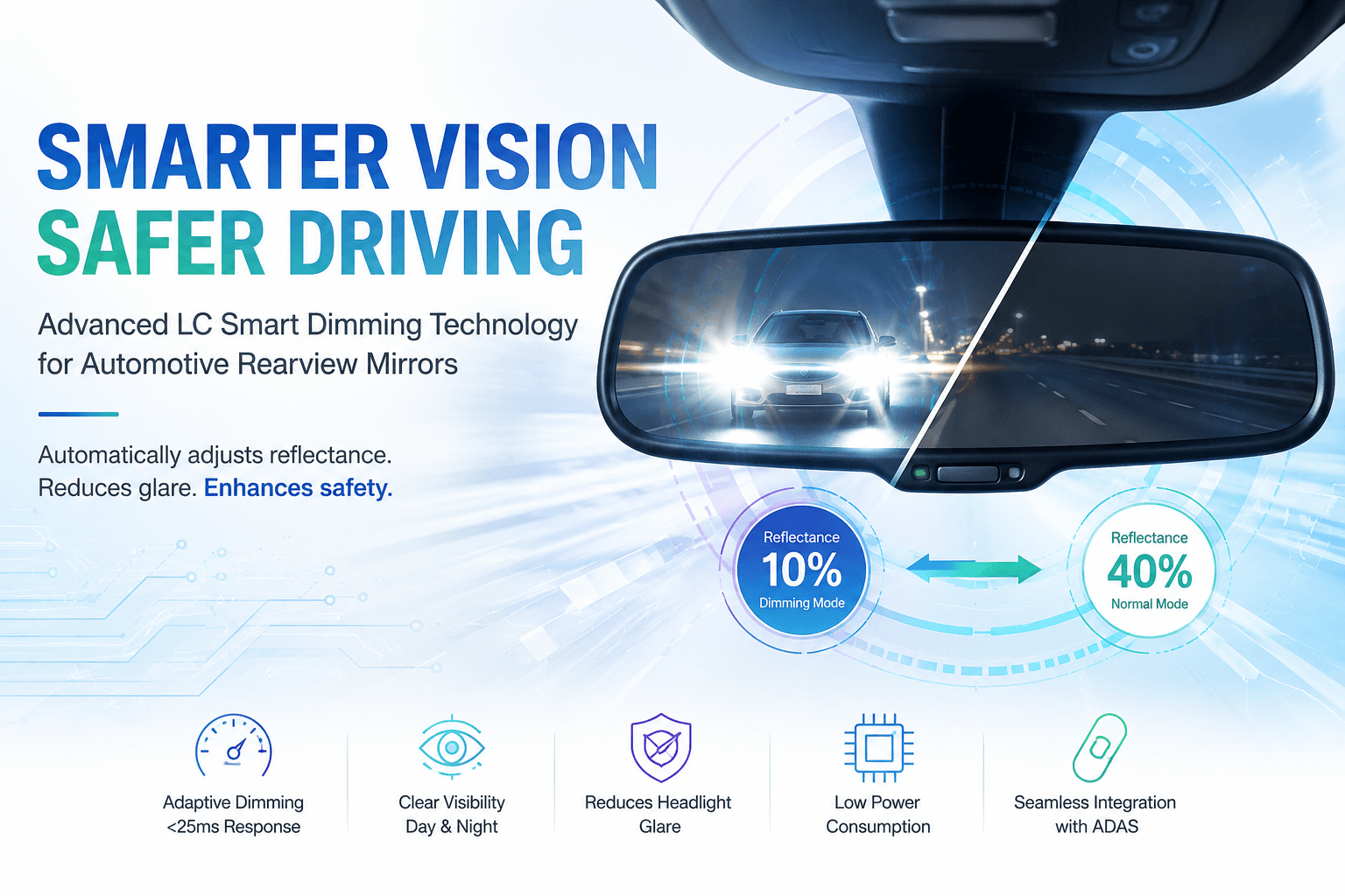
Our solution further enhances this performance by integrating Liquid Crystal (LC) smart dimming technology. Under normal driving conditions, the mirror provides clear visibility. When the system detects a potential glare hazard—such as intense headlights from a vehicle behind—it automatically switches to a dimming mode, reducing the mirror reflectance to approximately 10%. This significantly suppresses glare while maintaining sufficient rearward visibility, improving both driving comfort and safety during nighttime operation.
Regulatory Requirements
| Country/Region | Main Regulation / Standard | Application Scope | Minimum Mirror Reflectance Requirement | Remarks |
| Europe (EU) | UNECE Regulation No.46 (R46) | Interior/exterior rear-view mirrors and indirect vision systems | ≥40% | The primary regulation in Europe; electrochromic auto-dimming mirrors are allowed to reduce reflectance at night. |
| United States | FMVSS 111 | Rear visibility mirrors | Industry products commonly achieve 60–85%) | Focuses more on field of view and mirror performance; unlike UNECE R46, FMVSS 111 does not define a single universal reflectance requirement for all mirrors. |
| Canada | CMVSS 111 | Rear-view mirror systems | Generally follows North American FMVSS requirements | Requirements are similar to those in the United States. |
| China | GB 15084 Performance and Installation Requirements of Indirect Vision Devices for Motor Vehicles | Interior and exterior rear-view mirrors | ≥40% | Requirements are largely aligned with UNECE R46 |
| Japan | JIS / Road Vehicle Safety Standards (aligned with UNECE regulations) | Rear-view mirrors | ≥40% | Requirements are largely aligned with UNECE R46 |
| South Korea | KMVSS (Korean Motor Vehicle Safety Standards) | Rear-view mirrors | ≥40% | Requirements are largely aligned with UNECE R46 |
| Australia | ADR 14 | Rear vision mirrors | ≥40% | Requirements are aligned with UNECE R46. |
| Mexico | NOM-related regulations | Rear-view mirrors | Approximately ≥40% | Requirements are generally close to the North American market. |

Most global automotive rearview mirror regulations are harmonized around a minimum reflectance requirement of approximately 40%, with UNECE R46 serving as the primary reference standard. In practical mass-production applications, conventional glass mirrors typically achieve 70–85% reflectance, while advanced technologies such as electrochromic (EC) mirrors, LC digital mirrors, and smart rear-view mirror systems require additional consideration of optical performance, glare reduction, and night-time visibility.
Smart Dimming: The Future of Automotive Rearview Mirrors
As the automotive industry moves toward digital cockpits, intelligent sensing, and software-defined vehicles, rearview mirrors are evolving from passive reflective components into smart optical systems.
Compared with conventional fixed-reflectance mirrors, Liquid Crystal (LC) smart dimming technology offers several advantages:
- Fast response (<25ms) to changing lighting conditions
- Continuously adjustable reflectance for optimal driver comfort
- Reduced headlight glare during nighttime driving
- High optical clarity under daytime conditions
- Low power consumption and long service life
- Easy integration with ambient light sensors, cameras, and ADAS systems
By dynamically controlling mirror reflectance instead of relying on a fixed optical design, LC technology provides an optimal balance between visibility, safety, and driver comfort under all driving conditions.

Smart LC mirror with dimming function (right)
Conclusion
Mirror reflectance is one of the key optical parameters affecting driving safety. While international regulations generally require a minimum reflectance of approximately 40%, modern intelligent vehicles demand more than regulatory compliance—they require adaptive optical performance.
Liquid Crystal smart dimming technology enables rearview mirrors to automatically adjust reflectance according to ambient lighting conditions, significantly reducing glare without sacrificing image quality. As automotive displays and smart cockpit technologies continue to evolve, LC-based smart mirrors are expected to play an increasingly important role in enhancing both safety and the overall driving experience.
Looking for an advanced LC smart dimming solution for your automotive mirror application? Contact us to learn how our automotive-grade LC technology can help improve optical performance, driver safety, and user experience.
If you have any questions, please contact our engineering.
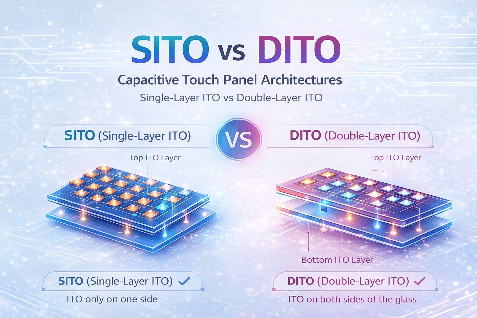
SITO vs DITO Touch Panel Architecture
Capacitive Touch detects touch by measuring changes in capacitance across a matrix of electrodes. Thus the core design question is: How do we arrange X and Y electrodes?
The two mainstream architectures in industry now are SITO (Single-layer ITO) and DITO (Double-layer ITO).
The core difference lies in whether the ITO is formed on both sides of the glass (DITO) or only on one side (SITO).

The red shadow in the image above indicates the ITO layer
DITO is patented by Apple and offers lower cost. For international customers, it is generally necessary to avoid using DITO.
SITO does not mean there is only a single ITO layer. It can also have multiple ITO layers. For example, in the case below, it is a SITO structure but includes two ITO layers (and it can have even more). The transmitter (Tx) and receiver (Rx) electrodes can be implemented on the same layer or on different layers, and there can also be additional jump/bridge layers.
Below is the 3D image show the SITO structure:

For a SITO design, both X and Y electrodes are implemented on a single ITO layer
SITO integrates both Tx and Rx electrodes on the same surface, which requires careful pattern design and layer management to ensure proper electrical isolation while maintaining stable capacitive coupling. In practice, SITO does not imply a single ITO layer; multiple conductive layers can be implemented on the same side by introducing insulating layers in between, allowing Tx and Rx to be arranged either on the same layer or on different stacked layers.
To achieve routing without electrical interference, additional structures such as bridges or jumpers are often used, enabling signal lines to cross over one another within a compact layout.
See below:

On the left, each diamond-shaped electrode represents an individual sensing unit, with the Tx and Rx electrodes arranged in an interleaved pattern through these diamond structures. Since all electrodes are located on the same side, direct routing would inevitably lead to signal lines blocking or intersecting each other. This is where the crossover structure becomes necessary. The positions labeled “crossovers” in the diagram are typical bridge points.
A bridge (or jumper) essentially works by locally elevating one signal line to cross over another. In practice, this is achieved by first forming a routing line on the bottom ITO layer, then covering it with a dielectric (insulating) layer, and subsequently adding a short conductive bridge on top (which can be made of ITO or metal). This allows the signal to “pass over” the other line before returning to the original layer. By separating the lines vertically in this way, electrical shorting is avoided.
Compared with DITO, SITO offers greater flexibility in avoiding patent constraints and is more suitable for global markets; however, it comes with increased process complexity, placing higher demands on alignment accuracy, dielectric uniformity, and yield control of bridge structures, while also requiring careful optimization between optical performance and electrical characteristics.
On the right, DITO can be understood as a structure in which the Tx and Rx electrodes are physically separated onto two different sides of the substrate, typically on opposite surfaces of the glass. In the “Two Layers Design” illustration, this separation is conceptually similar: the electrodes are distributed across different layers, so routing conflicts are inherently avoided.
Unlike SITO, where all electrodes share the same side and require bridge or jumper structures to cross over one another, DITO achieves this separation naturally by placing one set of electrodes (for example, Tx) on the top surface and the other set (Rx) on the bottom surface. As a result, there is no need for local crossover structures, since the signal lines do not compete for space within the same plane.
This architecture simplifies the pattern design and reduces process complexity related to bridge formation, dielectric deposition, and alignment of multi-layer routing on a single side. It also improves electrical performance consistency, since there are fewer discontinuities such as bridge transitions. However, DITO requires double-sided processing, including alignment between the two surfaces of the glass, which introduces its own manufacturing challenges.
If you have any questions, please contact our engineering.
How to Analyze I2C Waveforms
I2C is the most commonly used communication protocol in CTP systems. When customers report touch issues, we often use an oscilloscope to verify whether the CTP is functioning properly. Understanding how to analyze I2C waveforms is therefore essential for problem diagnosis and effective technical communication with customers.
Background of I2C
I2C (Inter-Integrated Circuit) was originally developed by Philips in 1982 for communication between its internal chips. The original specification supported speeds up to 100 kHz with 7-bit addressing. Although 7-bit addressing allows up to 128 addresses, some are reserved, so only 112 valid device addresses can be used on a bus.
In 1992, the first public specification introduced 400 kHz Fast Mode and extended 10-bit addressing. In many systems (for example, Arduino-compatible boards using the ATmega328 microcontroller), I2C support typically remains at Standard Mode (100 kHz) or Fast Mode (400 kHz), with either 7-bit or 10-bit addressing. Higher-speed modes (1 MHz to 5 MHz) exist but are less common.
*Serial vs Parallel Communication
Serial communication (e.g., I2C, UART, SPI, USB) transmits one bit at a time over a single data line in time sequence.
Data for I2C is typically as:
Clock
1 0 1 1 0 0 1 0 // I2C will transmit these data one bit by one bit
Parallel communication (e.g., MCU parallel bus, RGB interface) transmits multiple bits simultaneously in one clock cycle.
Data for RGB is typically as:
D7 D6 D5 D4 D3 D2 D1 D0
1 0 1 1 0 0 1 0 // 8 bits are transmitted in one clock cycle.
I2C Bus Architecture

I2C supports multi-master and multi-slave configurations and operates in half-duplex mode.
Customers often mention the term “node.” A node refers to any device connected to the I2C bus that has a valid address and is capable of communication. A node can function as either a master or a slave device.
A slave device, such as our Touch IC, cannot initiate communication. It can only respond to requests from the master. The slave must recognize its own address and will respond only when the received address matches its configured address.
For example, assume three slave devices have addresses 0x1A, 0x2A, and 0x3A. When the master transmits 0x2A on the SDA line, the second slave compares the received address with its own. If the address matches, communication is established.
Although all slave devices can detect the address transmitted by the master, only the device with the matching address will respond by sending an ACK (0). The others will ignore the transaction (NACK = 1). Each device address must be unique and is typically determined by hardware configuration. Examples will be provided later.
Half-duplex means that data can flow in only one direction at a time — either from master to slave or from slave to master. The data direction is controlled by the R/W bit.
In the I2C bus, SCL is the clock line and is always generated by the master. SDA is the data line and uses an open-drain structure, meaning it can be pulled low by either the master or a slave device.
Open-Drain Structure
What is an open-drain (or open-collector) structure? This type of output driving method enables bidirectional communication on a single data line in I2C systems.
An open-drain output can actively pull the signal line low or remain in a high-impedance (Hi-Z) state, but it cannot actively drive the line high. In contrast, a push-pull output can actively drive the signal either high or low.
When multiple devices are connected in parallel on the same bus, push-pull outputs may cause signal conflicts or even short circuits if different devices attempt to drive the line to opposite logic levels at the same time.
Push-pull output uses complementary PMOS and NMOS transistors to determine whether the output drives a high level (VDD) or a low level (ground).

High Level

Low Level
In an open-drain output structure, the PMOS transistor is permanently turned off (disconnected).
The circuit can either drive a low level (when the NMOS is turned on and conducts) or remain in a high-impedance state (when the NMOS is turned off).

Low Level

High-impedance state
When an external pull-up resistor is connected, the value of the pull-up resistor will appear at the output. PN-MOS itself are two diode2, with essentially infinite resistance.)

Open-Drain structure with a pull-up resistor
Only after understanding what open-drain outputs and pull-up resistors are can we better interpret the waveforms of SCL and SDA. In theory, SCL should be a regular square wave with very clean rising and falling edges.
In practice, for normal SCL and SDA waveforms, the falling edge is fast and sharp because the pull-down is active. The rising edge, however, is slower and curved or sloped because the voltage is pulled up through a resistor charging the line’s capacitance


As in the photo above, the yellow SCL line has a very slow rising edge, which is usually caused by a pull-up resistor that is too large.
Generally, for 100 kHz I²C, a 4.7 kΩ pull-up resistor is recommended, and for 400 kHz, 2.2 kΩ. If the pull-up resistor is too large, it can sometimes cause the touch sensor to become unresponsive.
A smaller pull-up resistor results in faster rising edges and stronger noise immunity, but it also increases power consumption.
I2C Data Format

Start and Stop Conditions

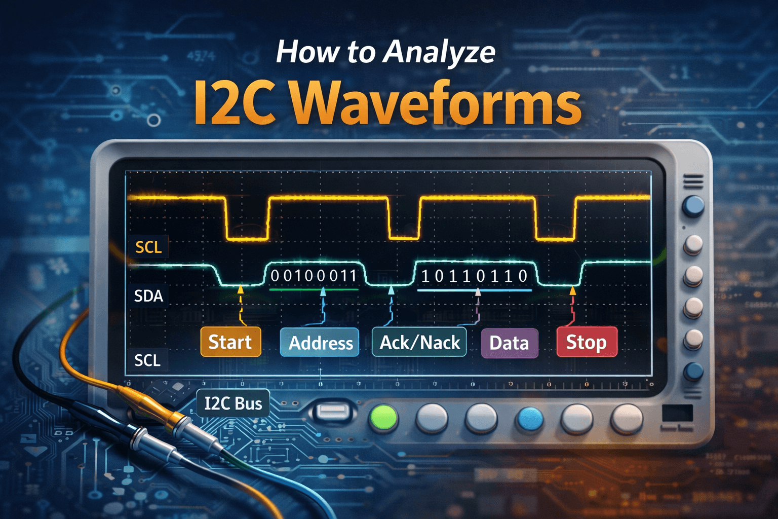
When SCL is high: SDA transitioning from high to low indicates a START condition; SDA transitioning from low to high indicates a STOP condition.
Addressing
An address frame typically consists of a 7-bit address plus 1 R/W bit (0 = write from master to slave, 1 = read from slave to master).
SDA must change only when SCL is low. During SCL high, SDA must remain stable because data is sampled during the high period of SCL.
In the diagram below, we can see that the slave’s A1, A2, and A3 pins are all connected to ground. This makes the address 1110000, which is 0x70 in hexadecimal.
Some devices, however, do not have A1, A2, and A3 address pins. In that case, the address cannot be changed and is fixed as a default internal static address.

ACK / NACK
After every 8 bits of data, the 9th clock cycle is used for ACK/NACK. The receiver drives SDA: ACK = 0 (acknowledge), NACK = 1 (not acknowledged).

A short pulse may appear between the 8th bit and the ACK bit. This occurs when the SDA line is released during direction switching. Because this transition happens while SCL is low and data is sampled during SCL high, this short pulse is not interpreted as valid data.
If you have any questions, please contact our engineering.
LCD Power-on Process
LCD Power-On Process
As LCD engineers, we often receive the following question: Why does a display occasionally show a white screen during power-on, while under other conditions it initializes and operates normally?
At first glance, it may appear that there is a problem with the display. However, in most cases, the issue is related to power sequencing and initialization timing. In other words, it is more of a software or system-level timing issue rather than a hardware defect.
To better understand this phenomenon, we need to review the LCD power-on process from a system-level perspective.
What Happens During Power-On?
A display contains a driver IC, internal logic circuits, voltage generation circuits, and timing detection circuits.
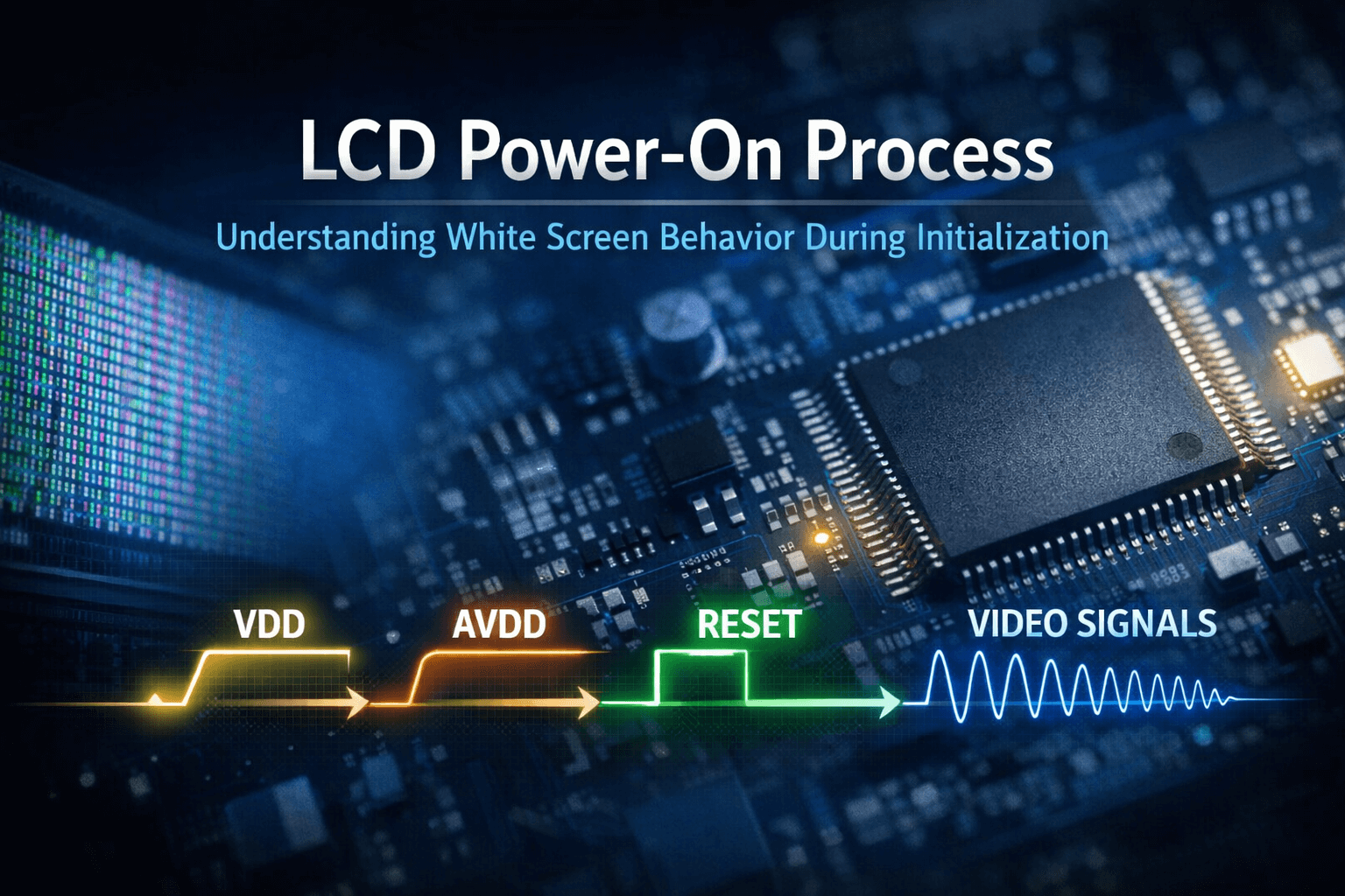
When the display is powered on, the following sequence must be strictly followed:
- The digital logic power supply (VDD) rises.
- The analog driving voltages (AVDD, VGH, VGL) are established.
- The RESET signal is applied and then released.
- The host MCU begins transmitting video signals, including clock, sync, and pixel data.
If any of these steps fail or occur out of sequence, the panel may not initialize correctly.
When a white screen is observed, it does not necessarily mean that the display is defective.
In most cases, it indicates that the TFT driver IC is not operating in its normal image refresh state.

Possible Root Causes of a White Screen
-
The Source Driver Outputs a Default Voltage Level
Under normal operation, the driver IC converts digital pixel data into analog driving voltages. These voltages control the liquid crystal orientation, resulting in different light transmittance levels for each pixel.
If the driver IC has not completed initialization, has not detected valid timing signals, or has not received valid image data, it may enter a default output mode. In this mode, the output voltage typically corresponds to a fully open liquid crystal (LC) state, which results in a uniformly white screen.
-
No Valid Image Data Is Latched
The driver IC requires continuous timing signals to correctly latch pixel data. These signals include:
- Pixel clock
- HSYNC
- VSYNC
- Data Enable (DE)
If no valid image data is latched, the display may show a uniform white screen.
-
The TFT Driver IC Did Not Complete Initialization
During power-on, the driver IC requires time to:
- Stabilize internal analog voltages
- Establish gamma reference levels
- Start internal oscillators
- Exit standby or sleep mode
- Initialize internal logic blocks
If the RESET signal is released too early, or if video data transmission begins before initialization is complete, the driver IC may enter an undefined state. In such cases, it may output the default voltage level, resulting in a white screen.
This is the most common cause observed in practical applications.
-
Pixel Clock Synchronization Failure
If pixel clock synchronization fails, the driver IC cannot correctly latch pixel data. In this case, the display may exhibit:
- A white screen
- A fully bright or fully dark screen
- Corrupted images
- Flickering
- Vertical or horizontal stripes
- Misaligned lines
Conclusion
A white screen is usually not a display hardware failure.
If the panel is powered and the backlight is functioning, the hardware is operational. However, the initialization sequence may have been incomplete, incorrectly ordered, or mistimed.
Therefore, debugging should focus on verifying: Power sequencing, RESET timing, Initialization delay requirements, Valid timing, and video signal transmission.
If you have any questions, please contact our engineering.
Understanding the Relationship Between Touch IC Driver, Firmware, and Configuration
When working with a Capacitive Touch Panel (CTP) software engineering team, we often refer to the terms Driver, Firmware (FW), and Configuration. These three concepts are not only discussed during the design phase, but are also repeatedly involved in later stages such as testing and validation.
Understanding the relationship and differences between them is fundamental to carrying out our related work effectively.
Recently, one of my customer asked: is it possible that different Touch ICs can use a same driver. Well, as an engineer, I fully understand the reason behind this question. If we can use one driver on different touch ICs, it will greatly reduce the development effort, maintenance cost and overall system complexity.
This article may be helpful for you to understand the relationship between driver, firmware and configuration, and answer the question above.
-
Driver
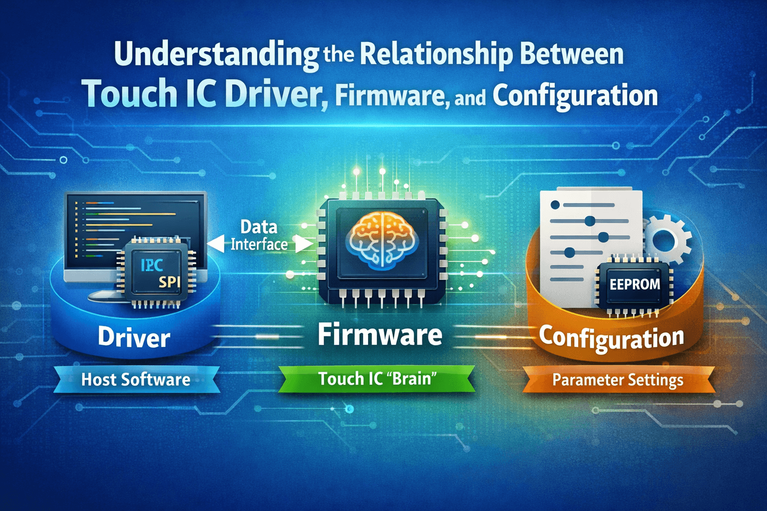
A driver is a host-side software that enables on the operating system (for example, Linux / Android / RTOS) or main controller to communicate with a hardware device. In a touch system, the driver is responsible for handing the communication protocol (such as I2C or SPI), reading and writing registers, parsing touch data, and reporting touch events to the system. The driver is a bridge between the host and the hardware, here, is the touch.
-
Firmware (FW)
Firmware (FW) is the software that run on the internal MCU of the touch IC and controls its core functions and behavior. In a touch system, the firmware determines how the touch IC works want what data it output. It can capture the touch signals, execute touch algorithms, manages TX/RX channels, and defines the data format.
Here, you may notice the most significant difference between driver and firmware. Driver always works on the host MCU, it is on the host side; while firmware runs on the touch IC. In a word, the driver helps the host to understand and receive the touch date, it is the “translator” between the MCU and the touch IC. While, firmware is the “brain” of the touch IC, it tells the IC what to do and how to do.
-
Configuration (Parameter Settings)
Different from driver and firmware, configuration itself is not a software, it is a set of parameters used to adjust how a touch IC operates, it provides the numerical and structural parameters that the firmware uses during operation. As a result, the same touch IC and firmware can work with different touch panels without modifying the touch algorithms*.
*What is algorithm logic? In one sentence summary, the algorithm logic are the firmware logic that converts the raw capacitive signals into accurate and reliable touch events. The algorithm logic determine whether a touch detected, where it is located, how many touch points are present.
*Here we can take a example to help you understand what a algorithm logic dose. Touch technology is widely used in kitchen appliances. For example, water droplets on an oven control panel can produce capacitive signals similar to a finger touch. The ability to tell water apart from a real finger touch depends on the touch algorithms.
Configuration is not code and does not contain any algorithm logic. It is stored in Flash of the touch IC, EEPROM, or sometimes it maybe also stored in the firmware. When the system turns on or initialization starts, firmware will read these parameters, and operate the touch algorithms based on these parameters. For example, there are two touch panels with different sizes and sensor patterns, however, we can use the same touch IC and firmware, this is achieved by setting up different configurations.
Now, let’s go back to our customer’s question: is it possible that different Touch ICs can use a same driver? The answer is yes. This is because a driver primarily depends on the communication protocol and data format. Do you remember, we have explain that the driver is the “translator” between the MCU and the driver IC. Same communication protocol and data format means they speak the same language. However, if the communication protocol is different, let’s say SPI and I2C, in this case, you will need two drivers. Normally, as long as the communication protocol and data format are consistent and the ICs belongs to the same series, the driver can be shared.
Should you have any questions, please consult our engineering.
Peck Model and Lifetime Evaluation: MTTF, MTBF, and Experimental Design
When evaluating the service life of a product, we often inform customers that the expected lifetime is 50,000 hours. However, this number is not derived from actual testing, but rather from theoretical calculations.
The method for measuring actual product lifespan is HALT (Highly Accelerated Life Test). HALT is a testing methodology that applies stress conditions far beyond normal usage—such as high/low temperatures, rapid thermal cycling, and vibration—to quickly expose potential weaknesses in a product. The primary purpose of HALT is not to determine the product’s exact lifespan, but to identify design flaws and early failure mechanisms, and to pinpoint which components are most susceptible to damage.
In practice, however, we more commonly use MTTF (Mean Time To Failure)-based evaluation strategies. MTTF is a quantitative reliability metric based on statistical lifetime distribution models (such as exponential or Weibull distributions). It estimates the average lifetime of a product by operating a set number of samples under standard or accelerated conditions, recording any failures over time.
The following table presents a real-world case we encountered. The accelerated aging model we used for analysis was the Peck model.

Introduction to the Peck Model
The Peck model is an empirical model used to predict the accelerated aging of electronic components and materials under the combined effects of temperature and humidity. Unlike the traditional Arrhenius model, which considers only temperature, the Peck model introduces a humidity exponent parameter, making it more suitable for simulating the impact of hot and humid environments on product lifetime. Its mathematical expression is:

Where:
- AF is the acceleration factor,
- RH is the relative humidity,
- n is the humidity exponent (typically ranging from 2 to 4; we use 3),
- E is the activation energy (commonly 0.7 eV for LCDs),
- k is the Boltzmann constant,
- T is the absolute temperature in Kelvin.
Using this model, the duration of an accelerated test can be converted into an equivalent lifetime under normal operating conditions.
For example, in our table, by substituting the following values:
RHtest: test relative humidity (90%)
RHuse: usage relative humidity (50%)
Ttest=333.15K
Tuse=298.15K
Ea =0.7eV
k=8.617×10⁻⁵ eV/K
n=3
AF=102.7
Equivalent Operating Time T=240hrs*102.7=24,648hrs.
Next, we need to substitute T into the MTBF formula.
Definition and Difference Between MTTF and MTBF
Both MTTF and MTBF are used to describe product reliability, but they apply to slightly different scenarios.
MTTF (Mean Time To Failure) refers to the average time a device operates before its first failure. It is applicable to non-repairable systems and represents the statistical expected lifetime, reflecting the reliability level of a product.
MTBF (Mean Time Between Failures) is typically used for repairable systems, and indicates the average operating time between two consecutive failures. For non-repairable systems (such as LCDs in our testing, which cannot be repaired once damaged), MTBF can be approximated as MTTF.
The formula for MTBF is as follows:

To calculate reliability from MTBF, the formula is as follows:

Experimental Design
Test Objectives:
Achieve the required MTBF lower bound corresponding to a 10-year lifetime, with both 5-year and 10-year reliability exceeding 90% under known conditions.
Equivalent test time per unit: 24,648 hours (based on extrapolation from 240 hours at 60°C / 90% RH using the Peck model).
Confidence levels: Sample size calculations for 90%, 95%, and 99% confidence levels.
Sample Size Requirements (Based on MTBF Reliability Calculation):
| Confidence Level | Samples for 90% Reliability @ 5 Years | Samples for 90% Reliability @ 10 Years |
| 90% | 39 | 78 |
| 95% | 54 | 101 |
| 99% | 83 | 156 |
Test Plan Details:
- Sample Size: Select based on desired reliability and confidence level; it is recommended to include a margin for contingency.
- Test Conditions: Continuous aging under 60°C / 90% RH for at least 240 hours (widely accepted industry standard).
- Data Monitoring: All failure events and times must be recorded throughout the test. If any failures occur, recalculate and adjust the plan accordingly.
- Periodic Assessment: After testing, use the Peck model to convert the test duration to equivalent lifetime. Evaluate MTBF and reliability using appropriate statistical methods.
- Risk Management: In case of failures, analyze the failure modes, adjust materials or processes, and optimize the design as needed.
Expected Conclusion:
If 78 samples are tested under 60°C / 90% RH for 240 hours, and no failures occur, the equivalent 10-year reliability of the product can be estimated at 90% (i.e., only 10% of units are expected to fail), which meets the general standard for consumer electronics (typically 80–90% reliability).
In contrast, if only 5 samples are tested (as shown in the initial table), the 5-year reliability would be just 43.9%, meaning that nearly half the units are expected to fail within 5 years—a conclusion that is not favorable for presentation to customers.
Contact our engineering team: tech@orientdisplay.com
Dual-Layer LCD Architecture Balancing Power Efficiency and Visual Performance
Introducing a Smarter Low-Power LCD Design for Small Home Appliances
In the ever-evolving world of smart appliances, power efficiency and user experience are equally vital. We’re excited to introduce our innovative dual-layer LCD solution, designed specifically for small home appliance applications that demand both high-resolution visuals and ultra-low-power standby modes.
The Architecture: Two Displays in One Panel
Our LCD module integrates two independent layers:
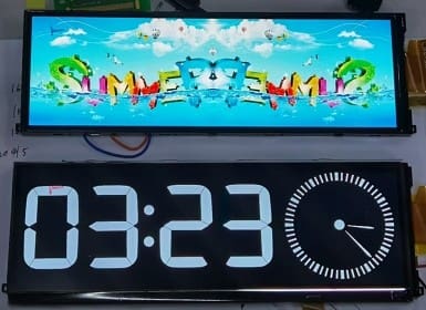
Upper Layer: Segment-type SVTN (VA panel)
Lower Layer: High-resolution IPS panel
This unique structure allows the device to switch seamlessly between high-performance display and low-power standby mode:
IPS Display (Active Mode):
When the device is in use, the vibrant IPS panel delivers a crisp, detailed user interface.
SVTN (VA) Display (Standby Mode):
When idle, the device shifts to the VA segment display. This layer consumes extremely low power, and can still display dynamic information like time, temperature, or status updates. To further reduce energy use, the backlight can be dimmed without losing visibility.
Why Not Use RAM-LCD ICs Instead?
While an alternative solution is to use a RAM-integrated LCD driver IC, that approach has several limitations:
- Static-only content unless the MCU frequently wakes up—leading to more power consumption.
- Software complexity increases significantly with real-time content.
- Higher BOM cost due to limited IC availability and premium pricing.
In contrast, our SVTN (VA) -based design is:
- Software-friendly: Minimal MCU involvement needed.
- Cost-effective: SVTN (VA) segments are simpler to drive, and component selection is broader.
- Power-efficient with dynamic capability.
Application Scenarios
Smart kettles, cookers, and humidifiers
IoT-enabled thermostats or timers
Battery-powered home gadgets requiring long standby time