

LCD Touchscreen Module Mura (Defect) and Solutions
What Mura is, how it is identified and graded, why optical bonding causes it, and how to reduce it.
On this page
“Mura” is the romanized spelling of the Japanese kanji “斑” (むら), which originally means unevenness, inconsistency, or defects. Because Japan was an early leader in the LCD industry, “Mura” has become a widely used technical term. It refers to various visible artifacts caused by non-uniform brightness in display panels (LCD/OLED).
Key takeaways
- Mura is visible brightness non-uniformity in LCD and OLED panels, often seen as yellow spots after optical bonding.
- It is identified on black, white, or low gray-level images in a dark room and graded with ND filters.
- Bonding-induced stress that deforms the liquid crystal cell is a key back-end cause.
- Fixes include thicker or softer adhesive, thinner cover glass, laminated adhesive, lower bonding pressure, and low-shrinkage curing.
What Is Mura?
This issue can occur in televisions, smartphones, and automotive dashboards. Brightness non-uniformity (Mura) degrades the viewing experience, reduces the perceived premium quality of a product, and may even interfere with display performance or functionality.
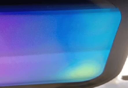
In the context of optical bonding, some manufacturers interpret Mura as light leakage. Because this defect may appear as yellow spots or yellowish lines along the edges of a white screen, many manufacturers also call it “yellowing.”
Mura Evaluation (Identification Method)
The simplest way to identify Mura is to switch the display to black, white, or low gray-level images in a dark room. By visually inspecting the edges around the active area (AA), you may observe irregular colors such as white, yellow, or other uneven patterns.
Viewing the display from different angles reveals various types of Mura, including stripes, patches, and clustered patterns, with no consistent color or shape. If pressure is intentionally applied to the display area, existing Mura intensifies, and it does not disappear immediately even after the external force is removed.
Given the working principle of liquid crystal displays, Mura is essentially unavoidable whenever stress is applied to the liquid crystal cell; it can only vary in severity.
Based on the principle of camera lens filters, Fujifilm developed ND (neutral density) filters. These filters come in eight levels: 1%, 2%, 3%, 4%, 5%, 6%, 8%, and 10%. In the industry, Mura is typically classified and evaluated according to these levels.
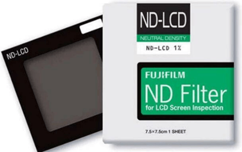
Neutral Density (ND) Filters
Among ND filters, a 1% transmittance filter (ND100) is more “stringent” (that is, it reduces light more strongly) than an 8% transmittance filter (about ND12).
The lower an ND filter’s transmittance percentage, the less light it lets through. It blocks more light and is therefore considered more “intense” or “stronger.”
A specific comparison:
- 1% transmittance (ND100): A strong ND filter, reducing light by about 6.6 stops. Suitable for daytime long-exposure photography, such as capturing flowing water with a silky effect.
- 8% transmittance (about ND12): A weak ND filter, reducing light by about 3.6 stops. Suitable for shooting in cloudy conditions or at dusk, with relatively mild light reduction.
In summary, the lower the transmittance percentage, the higher the ND value and the stronger the light reduction.
Causes of Mura
Mura can originate from materials or processes in the front-end manufacturing of the display panel, though specific solutions for those are not discussed here. It can also result from materials and processes used in back-end assembly.
This article focuses only on Mura that occurs after optical bonding. Assuming defects in the cover glass, panel, polarizer, backlight, and other materials have been ruled out, the discussion centers on Mura caused by deformation of the liquid crystal cell due to bonding-induced stress.
Typical examples include yellow spots and non-uniform display effects commonly observed after bonding.
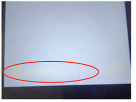
Failure analysis of defective units: A detailed teardown analysis was conducted on defective units. Removing the housing showed no change, and removing the backlight also produced no change. However, after the CTP (capacitive touch panel) and TFT were separated, the yellow spots disappeared. When the CTP was reattached and left to rest for several days, the yellow spots reappeared.
This confirms that the Mura defect in this case is related to the bonding materials or processes. In full-lamination processes, whether using OCA (optically clear adhesive) or liquid adhesive, Mura that appears after curing or after a period of rest is strongly related to adhesive selection and curing conditions.
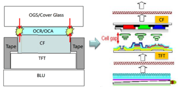
Impact of optical adhesive: Polymer-based adhesives tend to be relatively rigid. If the selected thickness is insufficient, their ability to absorb strain is poor. As a result, deformation stress reaches the liquid crystal layer and transmits mechanical distortion to the display. This creates non-uniformity in the liquid crystal cell gap, causing uneven light transmittance and, ultimately, visible color non-uniformity: Mura.
Solutions for Mura
Increase adhesive thickness
A thicker adhesive layer can absorb more deformation stress. However, this increases material costs, potentially even doubling them. Therefore, it is not recommended to use OCA with a thickness of 175 μm or thinner.
Reduce cover glass thickness
Thinning the cover glass can help reduce deformation. However, it may also decrease impact resistance and durability.

Use a softer adhesive (lower elastic modulus)
A softer adhesive can absorb stress better. However, if the adhesive is too soft, it may become difficult to handle during the bonding process.
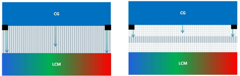
Use a laminated (multi-layer) structural adhesive
This type of adhesive combines the advantages of a thicker adhesive layer with improved stress absorption, and it offers the greatest improvement. A schematic diagram of stress distribution after bonding illustrates this advantage.
Reduce bonding pressure appropriately
Minimize lamination pressure where possible, assemble the backlight after bonding, and keep the bonding platform as flat as possible. This helps reduce excessive compression and potential damage to the liquid crystal cell.
Improve the shrinkage behavior of liquid adhesives
Select materials with lower curing shrinkage. Beyond changing adhesive materials, curing process parameters can also be optimized, for example with low-intensity, longer-duration UV curing or a gradual temperature ramp-up. These methods can help mitigate Mura to some extent.
If you have any questions, please contact our engineering team.
Frequently asked questions
What is Mura in an LCD or OLED display?
How do you identify and grade Mura?
What causes Mura after optical bonding?
How can Mura be reduced?
Can thin OCA be used for optical bonding?
New engineering articles by email.
Keep reading
TFT Displays
Display FundamentalsWhat Is an LCD and How It Works
Display FundamentalsLCD Viewing Angle, Viewing Direction, and Contrast
Cover Glass & CoatingsIntroduction to Cover Glass for Displays
Touch PanelsThe Evolution of Curved Touch Screens in Automotive Cockpits: From Aesthetics to True Flexibility
Enclosure & ReliabilityMethods for Securing TFT and OLED Display Panels in an Enclosure
Seeing Mura after optical bonding?
Talk to an engineer about adhesive selection and the bonding process for your display.