

Introduction to Embedded Touch Display Driver Chip (TDDI)
How TDDI combines touch and display driving in one chip, how it compares with GFF and on-cell structures, and its benefits for refresh rate and narrow bezels.
On this page
TDDI (Touch and Display Driver Integration) technology combines touch functionality with the display driver in a single chip, simplifying the display structure and enhancing performance. In TDDI technology, the touch sensor is typically integrated directly into the glass substrate of the display panel, creating an all-in-one touch and display solution.
Specifically, TDDI panels typically use a layer inside the cell, often the VCOM layer, as the touch sensor. This high level of integration enables both display and touch functionality in a streamlined form. This design makes the display thinner, reduces bezel width, improves the screen-to-body ratio, and simplifies the supply chain. The structure is as follows:
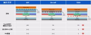
- The GFF (Glass-Film-Film) solution uses a separate structure for display and touch, where display and touch are independent modules.
- The On-cell solution embeds the touch sensor between the color filter substrate and the polarizer of the display screen, positioning the touch sensor on the display glass. This merges the display and touch modules into one, but the IC and FPC remain separate with two distinct designs.
- The TDDI solution fully integrates the touch sensor into the display’s TFT panel, unifying the display and touch modules, IC, and FPC into a single design. This is a highly integrated solution for display and touch functionality.
Due to its high level of integration, the TDDI solution offers benefits such as a thinner display, cost reduction, and a simplified supply chain. It has become the mainstream solution for LCD screens in smartphones. As of 2020, the LCD TDDI solution has accounted for over 50% of applications in smartphone display and touch functionality.
The development trends in smartphone TDDI display technology include high refresh rates, narrow bezels, and high functional integration.
(1) Advantages of High Refresh Rates
- Reduces flickering and jitter in image display, which helps alleviate eye strain.
- Enhances dynamic scenes in gaming applications, reducing blur and screen tearing during fast movements.
- Improves smoothness during screen transitions or scrolling, minimizing blurriness and ghosting in images and videos.
Requirements for TDDI IC: To support high refresh rates, TDDI ICs need faster MIPI data reception, higher oscillation frequencies (OSC), stronger drive capabilities, and faster response and processing speeds.
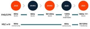
FHD LTPS TDDI: Production for 144Hz displays has been achieved, but 160Hz is still in the initial RFI (Request for Information) stage, with no corresponding products yet. Additionally, demand for LCD TDDI at 160Hz remains unclear, so most manufacturers are adopting a wait-and-see approach.
HD a-Si TDDI: Production has reached 90Hz, and a new recessed bump IC now supports 120Hz. For HD 120Hz displays, there are no technical bottlenecks or additional costs. Once cost-compatible motherboard configurations become available, manufacturers plan to launch projects, potentially upgrading HD displays to 120Hz.
(2) Narrow Bezels and Ultra-Narrow Bottom Bezels for Full-Screen Design
Manufacturers are also pursuing ultra-narrow bezels, especially at the bottom, to achieve a truly full-screen experience.
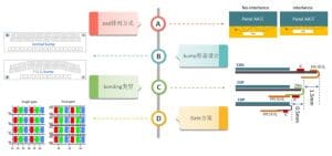
Narrow Bezel Technology Solutions:
- Pad Arrangement:
The interlace arrangement, compared to the no-interlace design, can reduce the bottom bezel by about 1mm without additional cost or performance impact. Thus, since 2017, interlace has replaced no-interlace as the mainstream choice. - Bonding Type:
The COF (Chip on Film) solution offers an advantage over COG (Chip on Glass) in terms of achieving narrower bezels. However, COF increases costs, making it less suitable for mid-to-low-end LCD models. Therefore, COG remains the primary bonding type for LCD TDDI solutions. - Gate Design:
Between 2018 and 2019, display and IC manufacturers introduced the dual gate design for HD a-Si displays to achieve narrower bottom bezels. However, as the dual gate design had performance issues and conflicted with the high refresh rate trend that emerged in late 2019, the market quickly abandoned it. Currently, the traditional single gate design dominates TDDI for smartphones. - Bump Design:
Following the discontinuation of the dual gate approach, glass manufacturers proposed a new recessed bump design to achieve narrower bezels. This design adds no extra cost and has no impact on other performance areas. It is expected to gradually replace the standard normal bump design, becoming the mainstream approach.
FHD LTPS: With a source demux design, the bottom bezel in the traditional normal bump configuration is already around 3.1mm. The reduction achieved by switching to recessed bump is minimal, so the demand for this change is not strong, and it remains in pre-research.
HD a-Si: The traditional normal bump design has a bottom bezel of 4.0-4.2mm, while the recessed bump design can reduce it to 3.0-3.2mm, achieving approximately a 1mm reduction. This approach is prioritized for HD products and is already in production for some smartphone models. Large-scale production is anticipated in the second half of 2022, with recessed bump expected to gradually replace normal bump as the mainstream solution.
Here are some major manufacturers of TDDI (Touch and Display Driver Integration) chips and examples of their products:
- Novatek:
- NT36525: Supports high-resolution displays, suitable for smartphones and tablets.
- NT36523: Designed for mid-to-high-end smartphones, featuring high refresh rates.
- FocalTech:
- FT8756: Supports Full HD (FHD) resolution, suitable for smartphones.
- FT8751: A cost-effective option for mid-to-low-end devices.
- Himax:
- HX8399: Supports high-resolution displays, suitable for smartphones and tablets.
- HX8394: Suitable for mid-range smartphones with good display performance.
- Solomon Systech:
- SSD2010: Supports a 454RGBx454 resolution, ideal for wearable devices.
- Chipone:
- ICNL9911C: Supports HD/HD+ resolution, suitable for smartphones.
- TDYTech:
- TD4160: Supports high refresh rates and multi-finger touch, suitable for smartphones and tablets.
- Synaptics:
- TD4303: Supports hybrid in-cell panel technology, suitable for smartphones.
These TDDI chips are widely used in smartphones, tablets, and wearable devices, offering high integration and excellent display and touch performance.
If you have any questions about Display and Touch Waterproofing Requirements, please contact Orient Display support engineers
Frequently asked questions
What is TDDI technology?
What are the benefits of TDDI?
How does TDDI differ from GFF and on-cell designs?
What are the development trends in smartphone TDDI?
How do TDDI displays achieve narrower bottom bezels?
New engineering articles by email.
Keep reading
Display Interfaces Explained
Design and IntegrationChoosing a Display Interface
Embedded DisplaysDisplay Controller and Driver ICs
Driver ICs & InterfacesWhy 0x29 Confuses Engineers: Packet Headers in MIPI DSI Explained
Driver ICs & InterfacesSPI Displays Are Not Video Streams: Understanding Command Mode LCDs
Driver ICs & InterfacesA Complete Guide to the Functions of Common Driving Voltages in TFT-LCD Display Modules
Have a display project in mind?
Talk to an engineer about the display your application needs.