
Displays

3M VHB Introduction

What it is VHB?

  • “VHB” stands for Very High Bond. The tape family is a line of double-sided acrylic-foam adhesive tapes that are designed to permanently bond parts without mechanical fasteners.
  • The 5952 version (as an example) has a 0.045 in (≈1.1 mm) thick black foam core with modified acrylic adhesive on both sides.
  • The foam core is “viscoelastic” — meaning it has both viscous (flows to fill gaps) and elastic (resists deformation) properties.
  • The tape is marketed as able to replace rivets, screws, welds, and liquid adhesives in many applications.

Key Features & Benefits

  • Strong bond + structural load capability: Because the adhesive flows into microscopic irregularities and the foam distributes load, you get both peel and shear strength.
  • Weather / environment resistance: The VHB tapes are designed for outdoor use, with resistance to UV, moisture, solvents, temperature cycling.
  • Flexibility / conformability: The viscoelastic foam helps accommodate differences in thermal expansion, slight mismatches in surface, and vibration.
  • Aesthetics & clean finish: Because you avoid visible screws, rivets, or welds, you can get smoother surfaces and cleaner appearance.
  • Simplified assembly: Compared to drilling, welding, screwing, etc., tape is faster and cleaner (no debris, no need to finish welds).

Typical Use-Cases / Applications

  • Construction & Architecture: Bonding exterior panels, metal to metal, glass to metal, etc. The tape distributes load across the full bond area rather than concentrating at fasteners.
  • Transportation: Automotive, trains, buses — where you might want to eliminate rivets or welds for weight savings, smoother surfaces, quieter ride (less vibration).
  • Appliances & Electronics: For joining dissimilar materials (metal, glass, plastics) where aesthetics and sealed bond is important.
  • Signage / Displays: Attaching signs, panels, trim where mechanical fasteners might be unsightly or impractical.

Selecting the Right Tape & Practical Considerations

  • Surface Energy / Material compatibility: Some versions are optimized for high and medium surface energy substrates (metals, glass, rigid plastics). Others target low surface energy plastics. For example, one guide says the “49” family is broad-range, “59” family for powder-coated plastics.
  • Surface Preparation: Critical for good bond. Cleaning, possibly abrasion or priming may be required, especially for plastics or low surface energy materials.
  • Pressure & dwell: After application you should apply firm pressure to get good contact of the foam to surface. Some load-bearing capacity builds over time as the adhesive flows.
  • Temperature limits: For example, 5952 allows short-term use up to ~300 °F (≈149 °C) and long-term up to ~200 °F (≈93 °C) on certain surfaces.
  • Thickness and tolerances: Foam thickness matters (gap-filling ability, bond line). For 5952 the thickness is ~1.1 mm ±10%.
  • Mechanical loads & environment: Though the tape is very strong, design should account for the loads (peel is always the worst for adhesives), possible expansion/contraction, vibration fatigue. The viscoelastic nature helps but you still need good engineering.
  • Removal / permanence: These tapes are intended to be permanent. Removal is difficult without damage to substrate.
  • Cost vs traditional fasteners: Tape may have higher material cost, but installation savings and appearance may offset. Also weight savings for transport applications.

Comparison Chart: Key Families

Family Key Features Typical Use-Cases Example Tape
4941 / 49xx Family General-purpose acrylic foam core; good adhesion to high & medium surface energy substrates (metals, glass, many plastics) with good conformability. Bonding panels, nameplates, trim, sign mounting on common substrates. 3M VHB Tape 4941
5952 / 59xx Family Modified acrylic adhesive + very conformable foam core; broader substrate range including powder-coated paints & many plastics. More challenging surfaces (paint, powder coat, some plastics), bonding dissimilar materials. 3M VHB Tape 5952
RP+ Family Premium version for high strength, large panels, dissimilar materials; good for structural bonding. Structural assemblies, large metal panels, where fasteners would normally be used. 3M VHB Tape RP+ 160GF
Clear / Thin Bond / Specialty Families Variants for aesthetic or specialized requirements: e.g., clear adhesive for glass/transparent parts; thin bond for minimal gap; flame-retardant, low VOC, LSE (low surface energy) plastics. Transparent assemblies, very thin or flush bond lines, bonding plastics with very low surface energy, electronics. Examples: 3M VHB Tape 4910 (clear); 3M VHB Tape 5906 (thin bond)


Example Product Variants

Here are some sample variants with different spec and intended uses:

  • 3M VHB Tape 5952: A common black-foam variant for many painted and powder-coated metals, good all-round.
  • 3M VHB Tape 4910 Clear: Clear version – for aesthetic applications where black foam not acceptable.
  • 3M VHB Tape 4611 High‑Temp: Higher temperature capability, suited for pre-paint bonding (metal assemblies).
  • 3M VHB Tape RP+ 160GF: Specialized for dissimilar surfaces and high temperature (e.g., up to ~450 °F short-term).
  • 3M VHB Tape 5958FR Flame Retardant: Flame-retardant version for building codes / electrical enclosures.
  • 3M VHB Tape 4941 General Purpose: General purpose version for many medium-duty applications.
  • 3M VHB Tape 4959 Heavy Duty: For heavier structural bonding, e.g., aluminum skin to steel frames in transportation.
  • 3M VHB Tape 5906 Thin‑Bond: Designed for thin bond lines – when you want minimal thickness between joined parts.

Limitations & Things to Watch

  • While tape is very strong, design still needs to account for peel stresses, differential expansion, and fatigue/vibration. Just sticking things together without considering loads can lead to failure.
  • Surface preparation is vital. Contaminants, insufficient priming, or low surface energy plastics can reduce bond strength significantly.
  • Temperature extremes: Although many versions resist high temps, extreme heat or cold beyond spec will degrade adhesive performance.
  • Bond line thickness: Too thick or too thin a gap may degrade performance. The foam core is chosen partly to compensate for irregular surfaces, but there are limits.
  • Disassembly or repair: If you need to remove or service bonded parts frequently, mechanical fasteners might still be better.
  • Cost & supply: Some VHB variants cost significantly more than standard tapes or mechanical fasteners. For large area bonding, cost-benefit must be considered.

How to decide which family/version to use

Here are some decision factors (especially relevant given your hardware systems work) and what to check:

  • Substrate Materials & Surface Energy
    • High/medium surface energy (HSE/MSE) materials like aluminum, steel, glass, many painted plastics → general-purpose tapes (e.g., 4941 family) often suffice.
    • Low surface energy (LSE) plastics, oily surfaces, powder-coated paints, “hard-to-stick” plastics → go for more specialized (59xx family, LSE versions)
    • If bonding dissimilar materials (e.g., metal to plastic), you might want the higher strength/conformability of RP+ or 59xx families.
  • Gap / Surface Irregularity / Thickness
    • If surfaces are perfectly flat and well matched, a thinner core (e.g., 0.4 mm) may work.
    • If surfaces are irregular or have mismatches (texture, gaps), a thicker or more conformable foam helps (e.g., 1.1 mm typical for many)
    • For very thin bond line requirements (minimal thickness between parts) the “thin bond” specialty versions are an option.
  • Mechanical / Environmental Loads
    • Consider shear vs peel forces: adhesive tapes handle shear (parallel to surface) much better than peeling (perpendicular) so design joint accordingly. The design guide explains this.
    • Temperature: If your bonded assembly sees high bake-cycles, ovens, high ambient temperatures, choose a tape rated for higher temperature (e.g., RP+ or specialty high-temp families)
    • Outdoor, UV, moisture, vibration: All VHB tapes have good durability, but the higher spec versions give more margin.
  • Aesthetics / Hidden Fasteners
    • If you want clean visible surfaces (no screws/rivets) then tape is excellent.
    • If the bond line must be invisible or clear (glass to glass, transparent plastics), use a clear version (4910 family or similar).
  • Serviceability / Future Removal
    • Adhesive tapes are intended as permanent bonds; if you expect to disassemble frequently, you may want mechanical fasteners or hybrid (tape + fastener) approach.
  • Surface Preparation & Application
    • Clean surfaces well (remove grease, oxide, contamination). Some surfaces may need abrasion or priming.
    • Apply sufficient pressure during bonding to ensure full contact. Some dwell time may be required to reach full strength.


Should you have any questions about VHB, please consult our engineering.

Displays

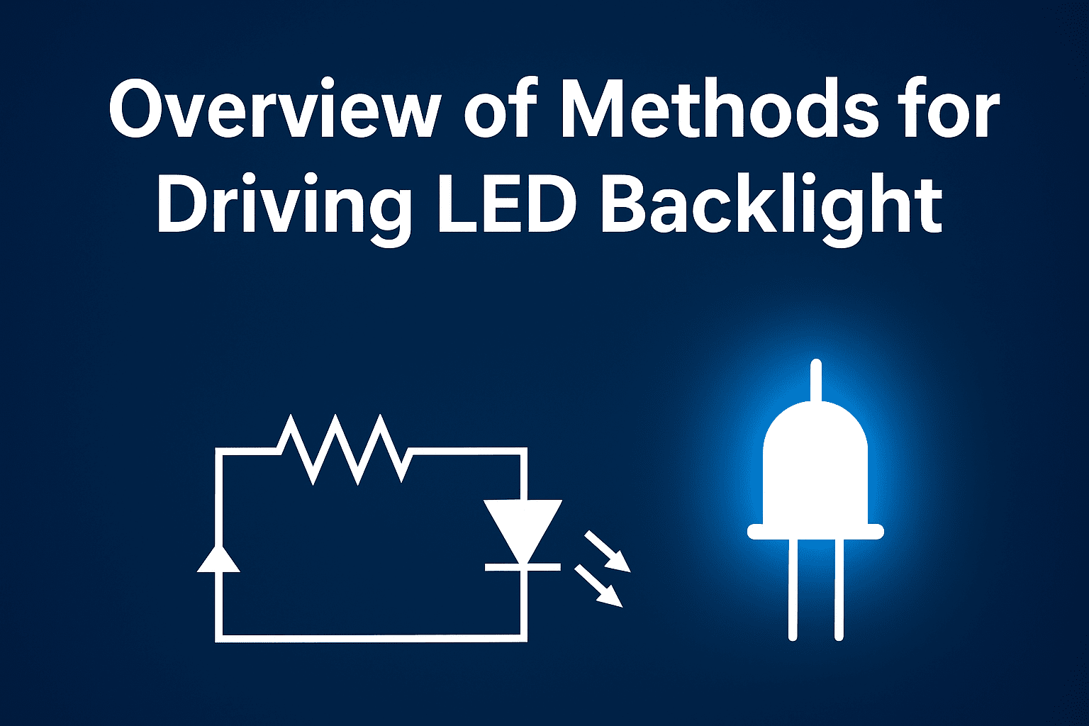
Overview of Methods for Driving LED Backlight

1. Operating Principle of LEDs

Before designing a driver circuit, it is important to understand how an LED operates. The brightness of an LED is primarily determined by its forward voltage (VF) and forward current (IF). The current–voltage characteristic curve is shown in Figure 1. Here, VF represents the forward voltage drop, while IF is the forward current.

Once the applied forward voltage exceeds the threshold level (also known as the turn-on voltage, approximately 1.7 V in this case), IF can be considered nearly proportional to VF. As illustrated in the figure, the maximum forward current of an LED can reach up to 1 A, while the typical forward voltage range is about 2 V to 4 V.


Figure 1. Relationship between VF and IF

The forward voltage drop of an LED can vary over a relatively wide range (more than 1 V). From the VF–IF curve shown above, it is clear that even a small change in VF can cause a large variation in IF, which in turn leads to significant fluctuations in brightness. For this reason, the luminous characteristics of LEDs are generally described as a function of current rather than voltage.

However, in typical rectifier circuits, the output voltage fluctuates with changes in the mains supply voltage. This means that using a constant-voltage source cannot ensure consistent LED brightness and may negatively affect LED performance. Therefore, LED drivers are usually designed to operate as constant-current sources.

2. LED Driving Techniques

From the operating principle of LEDs, it is clear that to maintain optimal brightness, an LED must be driven by a constant-current source. The driver’s role is not only to ensure this constant-current characteristic but also to achieve low power consumption.

To meet these requirements, the commonly used methods of current control include:

  • Adjusting the value of a current-limiting resistor to regulate the current.
  • Varying the reference voltage across the current-limiting resistor to control the current.
  • Using PWM (Pulse Width Modulation) to achieve current regulation.

The techniques employed in LED drivers are very similar to those used in switch-mode power supplies. In essence, an LED driver is a type of power conversion circuit, but its output is a constant current rather than a constant voltage. Under all conditions, the circuit must deliver a stable, average current, with ripple current kept within a specified range.

(1) Current-Limiting Method
Figure 2 shows the simplest circuit that uses the current-limiting method.


Figure 2. Simplest Circuit of the Current-Limiting Method

As shown in Figure 3, this is the traditional circuit configuration. The mains voltage is stepped down, rectified, and filtered, then a series resistor is used for current limiting to keep the LED operating stably and to provide basic protection.

However, the fatal drawback of this approach is that the power dissipated in the resistor R directly reduces system efficiency. Combined with transformer losses, the overall system efficiency is only about 50%. Moreover, when the supply voltage fluctuates within ±10%, the current through the LED can vary by 25% or more, and the power delivered to the LED may change by over 30%.

The main advantage of resistor current limiting is its simplicity, low cost, and lack of electromagnetic interference (EMI). Nevertheless, its disadvantages are significant: the LED brightness changes with variations in VF, the efficiency is very low, and heat dissipation becomes a serious issue.

Figure 3. Traditional Resistor Current-Limiting Circuit

There is also a straightforward article online about the current-limiting method that can be referenced: https://www.ourpcb.com/current-limiting-resistor.html

For more information on constant-current LED backlight driving, see: https://orientdisplay.com/wp-content/uploads/2018/07/OrientDisplay-Backlight-Constant-Current-Driver.pdf

(2) Voltage Regulation Method
As shown in Figure 4, this circuit is based on Figure 3, with the addition of an integrated voltage regulator (MC7809). This keeps the output voltage essentially stable at 9 V, allowing the current-limiting resistor R to be made very small, which prevents voltage instability across the LED.

However, the efficiency of this circuit remains low. Since the voltage drop across both the MC7809 and resistor R1 is still significant, the overall efficiency is only about 40%. To achieve both stable LED operation and higher efficiency, low-power current-limiting components and circuits should be used to improve system performance.

The linear voltage regulation method has the advantages of simple structure, few external components, medium efficiency, and relatively low cost.

Figure 4 Voltage Regulation Method

(3) PWM Method
PWM (Pulse Width Modulation) controls LED brightness by adjusting the duty cycle of the driving current pulses. This dimming technique repeatedly switches the LED driver on and off using simple digital pulses. By supplying digital pulses of varying width, the output current can be modulated, thereby changing the brightness of a white LED.

The distinctive feature of this driving circuit is that energy is transferred to the load through an inductor. Typically, a PWM control signal is used to switch a MOSFET transistor on and off. By varying the duty cycle of the PWM signal and the charging/discharging time of the inductor, the ratio between input and output voltage can be regulated.

Common circuit topologies of this type include buck, boost, and buck–boost converters. The advantages of the PWM method are high efficiency and stable performance, but its drawbacks include audible noise, higher cost, and more complex design.

Figure 5. LED Driving Circuit Using PWM Method

As shown in Figure 5, the PWM signal is connected through the base of transistor VQ1 to the gate of a P-channel MOSFET. The gate of the P-channel MOSFET is driven by a simple NPN transistor amplification circuit, which improves the MOSFET’s conduction process and reduces the power consumed by the driver circuit.

If the MOSFET is driven directly by the circuit, the rapid switching on and off of the MOSFET can cause oscillations in the drain–source voltage. This may lead to radio frequency interference (RFI) and, in some cases, expose the MOSFET to excessively high voltages, resulting in breakdown and damage.

To address this problem, a non-inductive resistor is inserted in series between the gate of the driven MOSFET and the driver circuit output. When the PWM signal is at a high level, transistor VQ1 conducts, pulling the MOSFET gate voltage below the source voltage. As a result, the MOSFET turns on, and the LED lights up. Conversely, when the PWM signal is at a low level, VQ1 is cut off, the MOSFET turns off, and the LED is extinguished.

3. LED Driver IC Solutions

LED backlight driver ICs are primarily used in LCD displays (televisions, laptops, mobile phones, automotive screens, etc.) to provide a constant current or constant voltage to the LED modules. Their purpose is to ensure uniform brightness, high efficiency, and long lifetime. Common driver topologies include boost (step-up), buck (step-down), buck–boost, and multi-channel constant-current drivers. Below are several representative categories of LED backlight driver ICs:

(1). Texas Instruments (TI)

  • TPS61169: Single-channel boost constant-current driver, suitable for small-size LCDs (e.g., mobile phones).
  • LP8556: Supports I²C control, multi-channel output (up to 6 channels), and both PWM/analog dimming. Widely used in laptops and automotive displays.

(2). ON Semiconductor (now onsemi)

  • NCP3170 / NCP3170B: High-efficiency buck drivers, suited for small- to medium-size screens.
  • NCV7685: 16-channel constant-current driver, often used in automotive backlighting and dashboards, featuring high reliability and diagnostic functions.

(3). STMicroelectronics (ST)

  • STLED524: Multi-channel LED backlight driver with I²C interface.
  • L5973D: Boost DC-DC converter for medium-power LED backlight systems.

(4). Renesas Electronics

  • ISL98611: Integrates boost and positive/negative charge pump outputs, designed for smartphone power and backlight driving.
  • ISL97900: Multi-channel LED backlight driver with high-precision current matching.

(5). China Manufacturers

  • Macroblock (MBI series): e.g., MBI5030, focused on large-display and backlight drivers, widely used in TVs and advertising panels.
  • Solomon Systech: Has released LED backlight driver solutions for mobile phones and small-to-medium displays.
  1. Summary
  • Small-size screens (phones, tablets): TI TPS/LP series, Renesas ISL series.
  • Medium-to-large screens (laptops, monitors, TVs): Multi-channel constant-current drivers such as TI LP8556, ST STLED524, Macroblock MBI series.
  • Automotive and industrial applications: Require reliability and multi-channel control, typically using onsemi NCV series.

4. Comparison Table of LED Backlight Driver ICs

Manufacturer Model Channels Driving Method Control Interface Typical Applications
TI (Texas Instruments) TPS61169 Single-channel Boost constant-current PWM / Analog Mobile phones, small displays
TI LP8556 6 channels Multi-channel constant-current with boost I²C + PWM Laptops, automotive displays
onsemi (formerly ON Semiconductor) NCP3170 Single-channel Buck constant-current PWM Small- to medium-size screens
onsemi NCV7685 16 channels Constant-current SPI / I²C Automotive backlight, dashboards
ST (STMicroelectronics) STLED524 6 channels Multi-channel constant-current I²C Monitors, televisions
ST L5973D Single-channel Boost DC-DC constant-current PWM / Analog Medium-power backlight
Renesas ISL98611 3 channels + power outputs Boost + charge pump I²C Smartphones, tablets
Renesas ISL97900 Multi-channel Constant-current I²C Laptops, tablets
Macroblock (明微电子) MBI5030 16 channels Constant-current SPI TVs, large advertising displays
Solomon Systech (晶门科技) SSD series (e.g., SSD2805) 6–8 channels Multi-channel constant-current I²C Mobile phones, small-to-medium displays

5. Key Parameter Comparison of LED Backlight Driver ICs

Manufacturer Model Input Voltage Range Output Channels Max Current (per channel) Efficiency Package Typical Applications
TI TPS61169 2.7–18 V 1 1.2 A ~90% SOT-23 Mobile phones, small displays
TI LP8556 2.7–5.5 V 6 30 mA ~90% WQFN Laptops, automotive displays
onsemi NCP3170 4.5–18 V 1 3 A ~90% SOIC-8 Small- to medium-size screens
onsemi NCV7685 6–40 V 16 75 mA ~85% TSSOP Automotive backlight, dashboards
ST STLED524 2.7–5.5 V 6 30 mA ~85–90% QFN Laptops, monitors
ST L5973D 4–36 V 1 2 A ~90% HSOP-8 Industrial / medium-power backlight
Renesas ISL98611 2.5–5.5 V 3 + power rails 30 mA ~90% WLCSP Smartphones, tablets
Renesas ISL97900 2.5–5.5 V 6 25 mA ~90% QFN Laptops, tablets
Macroblock MBI5030 3–5.5 V 16 80 mA ~85% SSOP/QFN Large TVs, advertising panels
Solomon Systech SSD2805 2.7–5.5 V 6–8 25 mA ~85% QFN Mobile phones, small-to-medium displays


Key Comparison Points

1.      Number of Channels

o   Small screens → Single-channel (e.g., TPS61169)

o   Medium screens / Automotive → 6-channel (e.g., LP8556, STLED524)

o   Large screens / Televisions → 16 channels or more (e.g., NCV7685, MBI5030)

2.      Driving Method

o   Boost (step-up) → Common in smartphones and tablets, used to raise low supply voltages to higher levels for driving multiple LEDs in series.

o   Buck (step-down) → Better suited for high-voltage power sources driving fewer LEDs.

o   Multi-channel constant-current → Ensures brightness uniformity, ideal for large-screen backlighting.

3.      Control Interface

o   PWM → Simple, widely used in mobile devices.

o   I²C → More flexible, allows adjustable current, voltage, and dimming curves.

o   SPI → High-speed and multi-channel, well-suited for TVs and advertising displays.


6. Recommended Application Scenarios for LED Backlight Driver ICs

  • Small-size screens (smartphones / tablets) → Single-channel boost drivers, e.g., TI TPS61169, Renesas ISL98611
  • Medium-size screens (laptops / automotive displays) → 6-channel multi-channel constant-current drivers, e.g., TI LP8556, ST STLED524, Renesas ISL97900
  • Large-size screens (monitors / TVs) → 16-channel or higher constant-current drivers, e.g., Macroblock MBI5030
  • Special scenarios (automotive / advertising displays) → High-reliability multi-channel drivers, e.g., onsemi NCV7685, Macroblock MBI series
author-avatar

About Veronica Chen

Technical Support - Orient Display

Displays

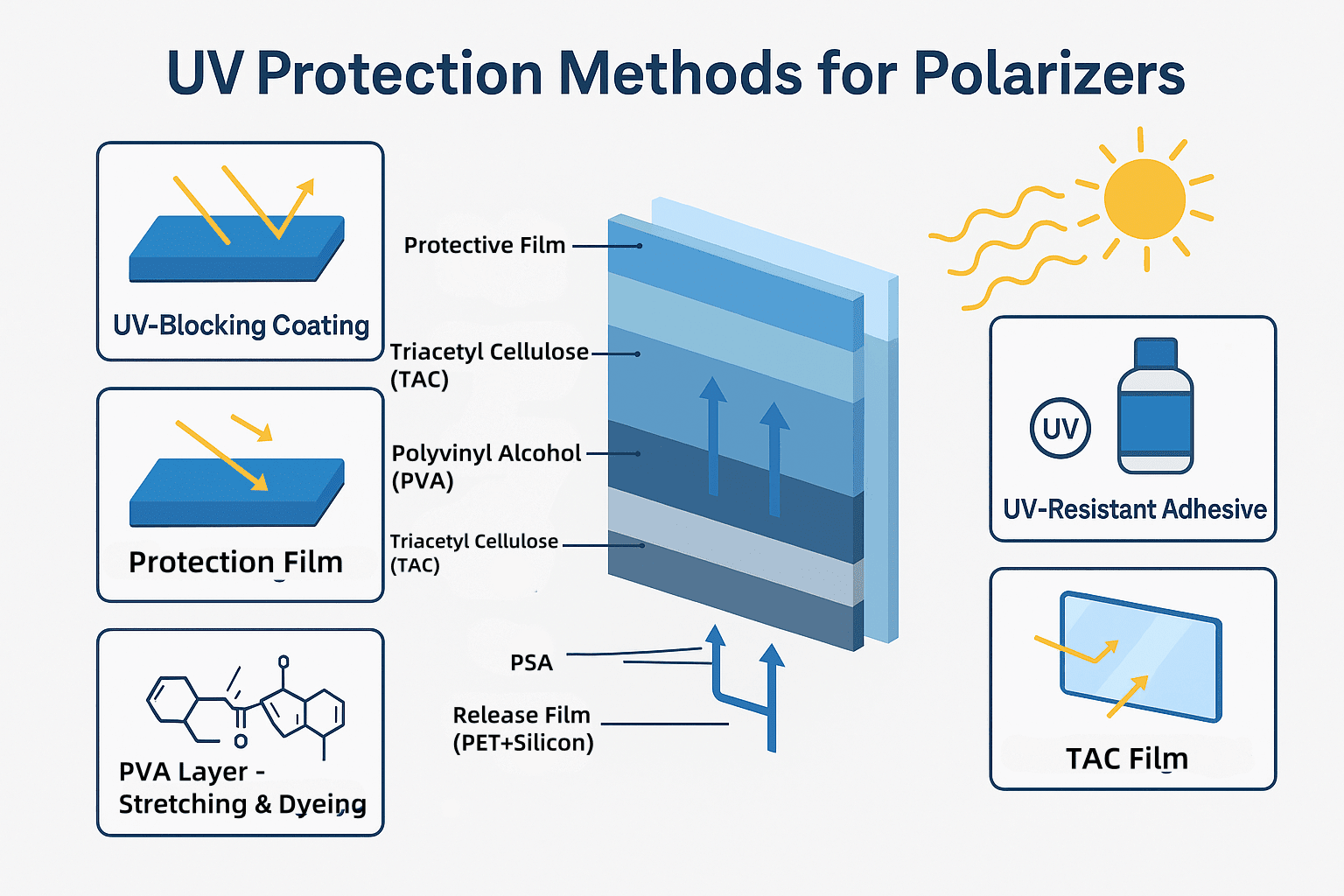
UV Protection Methods for Polarizers

Enhancing UV Resistance (100nm ~ 400nm) in Polarizers

Enhancing UV resistance (100nm ~ 400nm) is essential to prevent the polarizer layer from fading, degrading, yellowing, or failing due to ultraviolet exposure. Additionally, UV can damage the molecular structure of liquid crystals, leading to reduced performance. Once liquid crystal materials degrade, color deviation or yellow spots may occur, affecting display uniformity, image quality, and lifespan.

This time, we will focus on how to improve the UV resistance of polarizers.


Understanding Polarizer Structure and Process Flow

To understand how to enhance the UV resistance of a polarizer, we first need a basic understanding of its structure and manufacturing process.


General Structure of a Polarizer:

  1. Surface Coating:
    • Optional additional treatments.
    • Functional coatings applied directly to the surface of the TAC film.
    • Examples: Anti-scratch coatings (used in most polarizers), AR (Anti-Reflective), AF (Anti-Fingerprint), AS (Anti-Smudge), UV-blocking.
  2. Functional Film (Surface Protection Layer):
    • Optional additional film bonded to the TAC surface for enhanced performance.
    • Examples: Brightness enhancement film, UV protection, AF/AR/AS coatings, anti-static film.
  3. TAC Film (Triacetyl Cellulose) – Upper TAC:
    • Provides physical protection and structural support.
    • Protects the polarizer layer from scratches, moisture, oxidation, etc.
    • Offers mechanical strength and flexibility.
  4. PVA Polarizer Layer – Polyvinyl Alcohol:
    • The core functional layer.
    • After stretching, PVA molecules align with dye molecules, which selectively absorb light waves in a specific direction, thus achieving polarization.
  5. TAC Film – Lower TAC:
    • Symmetrical structure enhances mechanical strength.
    • Protects the underside of the polarizer layer.
  6. Pressure-Sensitive Adhesive (PSA) or Optical Clear Adhesive (OCA):
    • Bonds the polarizer to the LCD or touch panel glass.
    • Must remain transparent, bubble-free, and resistant to yellowing.
  7. Release Film or Protective Film

From this structure, it’s clear that the PVA polarizer layer is the most critical component. Therefore, to better understand how to enhance UV resistance, we must also understand the manufacturing process of the PVA polarizer layer.


PVA Polarizer Layer Manufacturing Steps

  • Dyeing:
    PVA is a water-soluble polymer. It is immersed in a solution containing iodine or organic dyes, which adhere to the film to form the polarizing material.
  • Stretching (Orientation):
    The dyed PVA film is stretched in one direction to align the dye molecules. These molecules selectively absorb light waves aligned with their direction, creating linearly polarized light. The transmitted light is perpendicular to the orientation of the dye.
  • Crosslinking Treatment (to enhance water resistance and stability):
    The stretched film is treated with chemical crosslinking agents such as boric acid and sodium ions to increase mechanical strength and moisture resistance.
  • Drying:
    The film is dried to remove excess moisture and stabilize the polarization effect.


Complete Production Flow of a Polarizer

Raw materials → Dyeing → Stretching → Crosslinking → Drying → Lamination → Cutting → Inspection → Packaging


Strategies to Enhance UV Resistance

Several structural and process-related measures can be taken to improve UV resistance:

  1. Surface Coating:

  • Apply UV-curable coatings containing UV protection components or nano UV shielding materials.
  • Provides a durable surface protection layer.
  1. Functional Protection Film:

  • Add UV barrier films (e.g., PET + UV coating) to further block short-wave UV rays.
  1. Upper and Lower TAC Films:

  • Use TAC films with UV absorbers to absorb UV rays (especially in the 280–400nm range), preventing penetration and protecting the internal PVA layer.
  • UV-absorbing or UV-reflecting coatings may also be applied to the TAC surface, especially in high-end applications.
  1. PVA Layer – Dyeing and Stretching:

Stretching Process:

  • During polarizer manufacturing, PVA films are dyed, then stretched to align dye molecules.
  • Unstretched PVA resembles tangled threads (random molecular chains), while stretched films have orderly aligned chains—like neatly combed hair—which control light direction.

How Stretching Enhances UV Resistance:

  1. Molecular Orientation Enhances UV Absorption (Indirect UV Protection):
    • Stretched PVA has highly ordered molecular chains, offering better light stability.
    • If UV-absorbing dyes are used (e.g., iodine-based), stretching aligns them for more effective UV absorption.
    • Even without dye, stretched PVA shows slightly enhanced UV absorption.
  2. Improved Structural Stability and UV Aging Resistance:
    • Stretching increases crystallinity and tightens molecular structure, improving UV durability.
    • Crucial for long-term exposure scenarios (e.g., outdoor sunglasses, automotive displays).
  3. Reduced Free Radical Pathways:
    • UV light excites unsaturated bonds in polymers, forming free radicals that cause degradation.
    • Ordered molecular structures reduce free radical diffusion, improving UV resilience.

Dyeing Process:

  • PVA alone absorbs little visible light—even after stretching—so polarization efficiency is low.
  • Dyes (like iodine) absorb light in specific directions and align with PVA chains during stretching to create high polarization efficiency (high transmission + high polarization).
  • Using UV-resistant, highly photostable dyes (e.g., special anthraquinone or azo dyes) prevents fading and extends lifespan.
  • Dye concentration must be controlled to avoid UV-accelerated degradation from overdosing.

Especially in LCDs, where high polarization performance is required, stretched dye films remain the most cost-effective and high-performance solution.

  1. Adhesive Layer (PSA/OCA):

  • Used to bond the two TAC films and the PVA layer.
  • Must be optically clear and durable.
  • Use optical adhesives with UV inhibitors to prevent yellowing, bubbling, or failure under UV.
  • Uniform coating/lamination without bubbles is critical to avoid UV leakage paths.


Summary: Key Points on UV Resistance in Polarizers

  1. UV radiation is the main external factor causing polarizer aging, especially for the PVA layer and dye structure. It leads to fading, breakage, contrast loss, and reduced display/module lifespan.
  2. UV resistance design involves both materials and structure:
    • Material level: Use TAC films, optical adhesives, and surface coatings with UV absorbers—mainstream absorbers include benzotriazole and triazine compounds.
    • Structural level: Stack UV-cut films or use UV coatings for enhanced shielding—especially critical for outdoor or in-vehicle applications with high UV exposure.
  3. Working principle of UV absorbers:
    • Convert UV energy into heat or harmless long-wave radiation, protecting the core PVA and dye layers from degradation.
    • UV cut performance is reflected in how well the entire structure limits UV (<400nm) transmission.
  4. Surface protection designs also play a key role:
    • Modern polarizers usually include a hard anti-scratch coating (HC).
    • Additional functional films (AR, anti-smudge, UV-blocking) may be added based on application needs vs. cost.
  5. System-level perspective:
    • Polarizers are just one part of the UV protection system.
    • Liquid crystals, light guide structures, and full module sealing are equally important.
    • UV resistance should be considered at the system design stage—for example, adding front-cover UV filter glass, using UV-resistant liquid crystal materials, etc.


Conclusion:

UV resistance is not just the task of a single material, but a multi-layered, multi-material system design strategy that directly affects the long-term stability and reliability of LCD displays.


author-avatar

About Veronica Chen

Technical Support - Orient Display

Displays

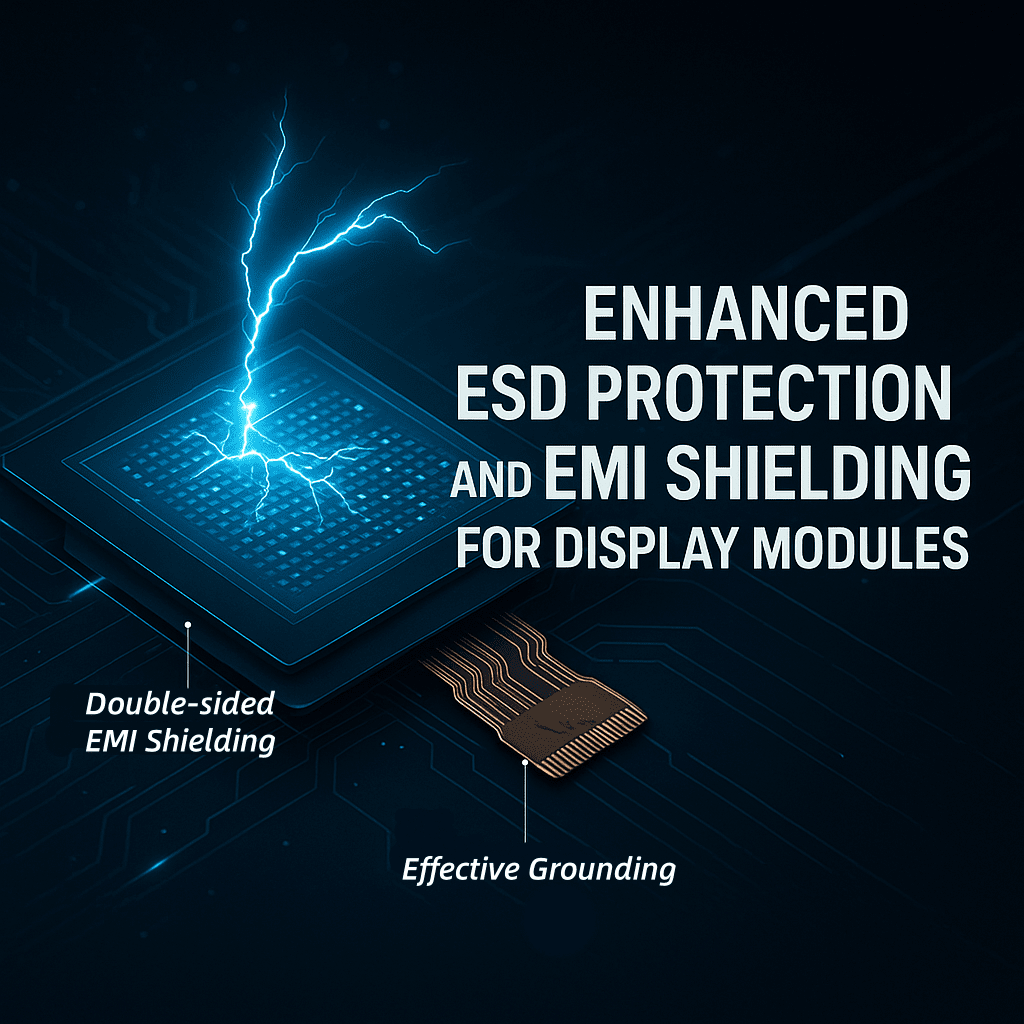
Enhanced ESD Protection and EMI Shielding for Display Modules

Key Reasons for ESD Requirements for Displays Becoming Increasingly Common

  1. Electronic Components Are Becoming More Precise and Sensitive

    As technology advances, the internal components of displays—such as integrated circuits (ICs), driver chips, and touch panels (TP)—are becoming more miniaturized and low-power. This makes them less tolerant to electrostatic discharge (ESD), where even a small static charge can cause functional abnormalities, shorten the lifespan, or directly damage the components.


  1. Applications Are Becoming More Diverse and Complex

    Display usage has expanded beyond traditional indoor environments to more demanding settings, such as:

  • Industrial equipment: frequent friction and dust accumulation easily generate static electricity
  • Medical devices: require high reliability and safety
  • Automotive systems: enclosed environments easily lead to electrostatic induction
  • Outdoor terminals: dry climates increase the risk of static charge build-up


  1. Widespread Use of Touch Technology

    As touch displays become more common, users frequently interact directly with the screen. In dry environments or when wearing synthetic fabrics, it is easy to generate static electricity. Discharge directly onto the touch surface poses a greater risk to circuit integrity, so enhancing surface-level ESD protection is essential.

Our standard TFT displays typically meet the following ESD protection levels:

  • Air discharge: ±8KV
  • Contact discharge: ±4KV

These are in line with the specifications described in our datasheets and are essential for ensuring product reliability.


  1. With increasing application demands and evolving environmental challenges, higher Electrostatic Discharge (ESD) protection levels are often required for display modules

particularly in industrial, automotive, and outdoor settings. When customers request enhanced ESD performance, such as:

  • Air Discharge: ±15KV
  • Contact Discharge: ±8KV


Recommended Solution: Double-sided EMI Shielding

Component: FPC Shielding Layer
Structure: Double-sided EMI (Electromagnetic Interference) Shielding Film

Description:

To improve the Electromagnetic Compatibility (EMC) of the display module, we recommend the use of a Double-sided EMI shielding structure. This design involves applying EMI shielding materials to both the front and back sides of the display module.

 Key Functions:

  • Effectively suppresses internal and external electromagnetic interference
  • Enhances the stability and reliability of signal transmission
  • Helps meet higher ESD immunity levels as specified in IEC 61000-4-2 standards


Additional Recommendations

In addition to the EMI shielding layer, further system-level measures can be considered

  • Grounding design optimization between module and enclosure
  • Use of conductive foam or gasket around the module perimeter
  • Application of anti-static coatings or films on exposed surfaces

EMI shielding material is like an “umbrella” that blocks interference.
Grounding wire is like a “drainpipe” that channels interference away.

Only by combining both can we achieve a true “shielding + discharge” integrated protection.

Examples of Common Grounding Methods:

Application Area Grounding Method
LCM metal backplate Connected to the mainboard GND point
Touch FPC shielding layer Grounded via GND pin or metal frame
Conductive foam/tape Attached to grounding copper foil or metal housing
EMI shielding sticker Connected to grounding point on housing or bracket


Signal Ground vs. Chassis Ground

Although both are referred to as “ground,” Signal Ground and Chassis (Physical) Ground have different purposes and characteristics in electronics:

Signal Ground (Logic Ground)

Purpose: Serves as a voltage reference for signal transmission (typically 0V)

Location: Internal circuit ground used by ICs, resistors, capacitors, etc.

Characteristics:

    • Used in logic and analog circuits
    • Not necessarily connected to the earth
    • Typically found in low-noise, low-current environments

Example: The GND pin of an MCU or sensor

Chassis Ground / Earth Ground

Used once the display module is integrated into the full device

Purpose:

    • Discharge static electricity (ESD) to prevent component damage
    • Reduce EMI via housing-level shielding
    • Improve EMC performance through unified grounding

Example: Metal frame, conductive tape, or backlight housing grounded to the device chassis


Summary

To meet elevated ESD requirements (±15KV air / ±8KV contact), both EMI shielding and effective grounding are essential.
By combining signal-level reference grounding with chassis-level discharge pathways, and by incorporating double-sided EMI shielding, we can ensure robust protection, greater product reliability, and compliance with industrial EMC/ESD standards.


Does your project have special requirements for ESD protection? Feel free to contact our engineer at <tech@orientdisplay.com>—we’re always happy to help.

author-avatar

About Lily Liang

Sales Manager - Orient Display

Displays

How to Estimate Battery Life for Your Device – Even with Sleep Modes

Whether you’re designing a sensor node, a wearable device, or a portable gadget, battery life estimation is a key part of the process. Here’s a simple way to calculate how long your battery will last — even if your device switches between active and sleep modes.

Basic Formula (For Constant Current)

If your device draws a constant current, battery life is easy to estimate:

Battery Life (hours) = Battery Capacity (mAh) / Device Current Consumption (mA)

Example:
– Battery: 2200 mAh
– Device current: 40 mA
Battery Life = 2200 / 40 = 55 hours

When Your Device Has Sleep and Active Modes

In most real-world applications, devices don’t run at full power 24/7. They might wake up briefly, do some work, then return to low-power sleep mode.

To account for this, you’ll need to calculate the average current draw across the full duty cycle (i.e., one full period of activity and sleep).

Step-by-Step Example

Let’s say your device:
– Draws 40 mA when active, and stays active for 2 seconds
– Draws 0.1 mA when sleeping, and sleeps for 8 seconds
– Total cycle = 10 seconds

Step 1: Compute Average Current
Average Current = ((40 * 2) + (0.1 * 8)) / 10 = (80 + 0.8) / 10 = 8.08 mA

Step 2: Estimate Battery Life
Using a 2200 mAh battery:
Battery Life = 2200 / 8.08 ≈ 272.3 hours

Real-World Considerations

While this gives a solid estimate, keep in mind:
– Battery capacity decreases with age and cold temperatures.
– Devices may consume extra current during startup, communication bursts, or sensor sampling.
– Battery cutoff voltage matters — some devices shut down before the battery is truly empty.

Final Tip

Use this method during your design phase to make informed decisions about battery size, duty cycles, and sleep strategies. Optimizing power usage can drastically extend your product’s life between charges.

If you’d like to make this easier, feel free to reach out — our engineers are happy to help.


Displays

Peck Model and Lifetime Evaluation: MTTF, MTBF, and Experimental Design

When evaluating the service life of a product, we often inform customers that the expected lifetime is 50,000 hours. However, this number is not derived from actual testing, but rather from theoretical calculations.


The method for measuring actual product lifespan is HALT (Highly Accelerated Life Test). HALT is a testing methodology that applies stress conditions far beyond normal usage—such as high/low temperatures, rapid thermal cycling, and vibration—to quickly expose potential weaknesses in a product. The primary purpose of HALT is not to determine the product’s exact lifespan, but to identify design flaws and early failure mechanisms, and to pinpoint which components are most susceptible to damage.


In practice, however, we more commonly use MTTF (Mean Time To Failure)-based evaluation strategies. MTTF is a quantitative reliability metric based on statistical lifetime distribution models (such as exponential or Weibull distributions). It estimates the average lifetime of a product by operating a set number of samples under standard or accelerated conditions, recording any failures over time.


The following table presents a real-world case we encountered. The accelerated aging model we used for analysis was the Peck model.


Introduction to the Peck Model

The Peck model is an empirical model used to predict the accelerated aging of electronic components and materials under the combined effects of temperature and humidity. Unlike the traditional Arrhenius model, which considers only temperature, the Peck model introduces a humidity exponent parameter, making it more suitable for simulating the impact of hot and humid environments on product lifetime. Its mathematical expression is:

Where:

  • AF is the acceleration factor,
  • RH is the relative humidity,
  • n is the humidity exponent (typically ranging from 2 to 4; we use 3),
  • E is the activation energy (commonly 0.7 eV for LCDs),
  • k is the Boltzmann constant,
  • T is the absolute temperature in Kelvin.

Using this model, the duration of an accelerated test can be converted into an equivalent lifetime under normal operating conditions.

For example, in our table, by substituting the following values:

RHtest​: test relative humidity (90%)

RHuse​: usage relative humidity (50%)

Ttest​=333.15K

Tuse=298.15K

Ea ​=0.7eV

k=8.617×10⁻⁵ eV/K

n=3

AF=102.7

Equivalent Operating Time T=240hrs*102.7=24,648hrs.

Next, we need to substitute T into the MTBF formula.


Definition and Difference Between MTTF and MTBF

Both MTTF and MTBF are used to describe product reliability, but they apply to slightly different scenarios.

MTTF (Mean Time To Failure) refers to the average time a device operates before its first failure. It is applicable to non-repairable systems and represents the statistical expected lifetime, reflecting the reliability level of a product.

MTBF (Mean Time Between Failures) is typically used for repairable systems, and indicates the average operating time between two consecutive failures. For non-repairable systems (such as LCDs in our testing, which cannot be repaired once damaged), MTBF can be approximated as MTTF.


The formula for MTBF is as follows:

To calculate reliability from MTBF, the formula is as follows:

Experimental Design

Test Objectives:

Achieve the required MTBF lower bound corresponding to a 10-year lifetime, with both 5-year and 10-year reliability exceeding 90% under known conditions.

Equivalent test time per unit: 24,648 hours (based on extrapolation from 240 hours at 60°C / 90% RH using the Peck model).

Confidence levels: Sample size calculations for 90%, 95%, and 99% confidence levels.

Sample Size Requirements (Based on MTBF Reliability Calculation):

Confidence Level Samples for 90% Reliability @ 5 Years Samples for 90% Reliability @ 10 Years
90% 39 78
95% 54 101
99% 83 156

Test Plan Details:

  • Sample Size: Select based on desired reliability and confidence level; it is recommended to include a margin for contingency.
  • Test Conditions: Continuous aging under 60°C / 90% RH for at least 240 hours (widely accepted industry standard).
  • Data Monitoring: All failure events and times must be recorded throughout the test. If any failures occur, recalculate and adjust the plan accordingly.
  • Periodic Assessment: After testing, use the Peck model to convert the test duration to equivalent lifetime. Evaluate MTBF and reliability using appropriate statistical methods.
  • Risk Management: In case of failures, analyze the failure modes, adjust materials or processes, and optimize the design as needed.


Expected Conclusion:

If 78 samples are tested under 60°C / 90% RH for 240 hours, and no failures occur, the equivalent 10-year reliability of the product can be estimated at 90% (i.e., only 10% of units are expected to fail), which meets the general standard for consumer electronics (typically 80–90% reliability).

In contrast, if only 5 samples are tested (as shown in the initial table), the 5-year reliability would be just 43.9%, meaning that nearly half the units are expected to fail within 5 years—a conclusion that is not favorable for presentation to customers.


Contact our engineering team: tech@orientdisplay.com

author-avatar

About Alex Wang

Technical Engineer - Orient Display