

Blog
Terminology and Comparison in Embedded System
Arduino
Arduino-Compatible Boards
These work with the Arduino IDE and libraries:
- Seeeduino (by Seeed Studio)
- Fully Arduino-compatible; often more compact or cheaper.
- Versions like Seeeduino Lotus include Grove ports for easy sensor integration.
- SparkFun RedBoard
- Same ATmega328P chip as Arduino Uno.
- Designed for better USB compatibility and robustness.
- Adafruit Metro
- Arduino Uno-compatible.
- Comes in ATmega328 or M0/M4 (more powerful ARM) variants.
- Elegoo Uno / Mega / Nano
- Cheaper clones of Arduino boards.
- Great for beginners or bulk classroom use.
More Powerful Microcontrollers
These offer more processing power or features:
- Raspberry Pi Pico / Pico W
- Based on the RP2040 chip (dual-core ARM Cortex-M0+).
- Programmable in MicroPython, C/C++, or via Arduino IDE (with configuration).
- Teensy (by PJRC)
- Very powerful (Cortex-M4 or M7); supports audio, real-time control.
- Arduino IDE compatible via Teensyduino add-on.
- ESP8266 / ESP32 (by Espressif)
- Built-in Wi-Fi (and Bluetooth for ESP32).
- Compatible with Arduino IDE and great for IoT.
Industrial / Educational Boards
These are designed for durability, education, or expanded use cases:
- Micro:bit (BBC)
- ARM Cortex-M0/M4; ideal for education.
- Has built-in sensors, LEDs, Bluetooth.
- STM32 Nucleo Boards
- Based on STM32 ARM Cortex-M microcontrollers.
- Arduino pin compatibility + STM32Cube ecosystem.
- Particle Photon / Argon
- Focused on cloud-connected IoT.
- Works with Particle Cloud and supports Arduino-like development.
Raspberry Pi
Direct Raspberry Pi Alternatives
- Banana Pi Series (e.g., BPI-M5, BPI-M2 Pro)
- ARM-based; similar form factor and GPIO layout.
- Often more RAM or better I/O, but software support can lag.
- Orange Pi Series (e.g., Orange Pi 5, Orange Pi Zero 2)
- Powerful Rockchip/Allwinner-based boards.
- Great specs for the price, but less mature OS/software support.
- Rock Pi Series (by Radxa) (e.g., Rock Pi 4, Rock Pi 5)
- Rockchip RK3399 or RK3588-based (much more powerful than Pi 4).
- Good performance and better AI acceleration than Raspberry Pi.
- Odroid Series (by Hardkernel) (e.g., Odroid-C4, Odroid-N2+, Odroid-XU4)
- ARM Cortex-A73/A55 or Exynos-based.
- Powerful, with good Linux support and active community.
- Libre Computer Boards (e.g., Le Potato, Tritium)
- Raspberry Pi-compatible form factor.
- Mainline Linux kernel support; focused on open-source.
More Powerful SBCs (Edge AI / Desktop Replacement)
- NVIDIA Jetson Series (e.g., Jetson Nano, Jetson Orin Nano)
- Built for AI and computer vision (CUDA/GPU acceleration).
- Ideal for robotics and ML projects.
- BeagleBone Black / AI-64
- More focused on real-time control and I/O (PRUs).
- BeagleBone AI-64 competes with Jetson and Pi 5 in power.
- UP Board Series (by AAEON)
- Intel x86-based SBCs.
- Suitable for industrial, Windows/Linux desktop, or edge AI.
Ultra-Compact Boards (Raspberry Pi Zero Competitors)
- NanoPi Series (by FriendlyELEC) (e.g., NanoPi Neo, NanoPi R5S)
- Tiny, affordable, with various performance levels.
- Great for headless IoT and embedded projects.
- LattePanda Series
- Intel Atom/x86 SBC with optional Arduino co-processor.
- Unique combo of PC power and microcontroller I/O.
STM32
Some microcontroller families that compete directly with STM32 (by STMicroelectronics), offering similar or better features depending on the application:
ARM Cortex-M Competitors
- NXP LPC Series (LPC800 / LPC1100 / LPC54000, etc.)
- ARM Cortex-M0/M3/M4/M33 cores.
- Known for low power and good USB support.
- Strong IDE support via MCUXpresso.
- Renesas RA and RX Series
- RA: ARM Cortex-M (RA2, RA4, RA6 with M23/M33).
- RX: Proprietary 32-bit core, high performance, low power.
- Industrial reliability and long-term availability.
- Nordic Semiconductor nRF52 / nRF53 Series
- ARM Cortex-M4/M33 with integrated Bluetooth Low Energy.
- Excellent for low-power wireless applications.
- Texas Instruments MSP432 / Tiva C Series
- MSP432: ARM Cortex-M4F, low power, high precision ADCs.
- Tiva C: ARM Cortex-M4, general purpose.
- Silicon Labs EFM32 Gecko Series
- ARM Cortex-M0+/M3/M4.
- Extremely low power (Energy Micro acquisition).
- Great for battery-powered devices.
IoT-Focused Chips with Wi-Fi/Bluetooth
- Espressif ESP32 / ESP32-S3 / ESP32-C6
- Dual-core or single-core RISC-V/ARM variants.
- Built-in Wi-Fi + BLE.
- Low cost, Arduino and MicroPython support.
- Raspberry Pi RP2040
- Dual-core Cortex-M0+ (not STM32 level in raw power).
- PIO (Programmable IO) is unique.
- Popular due to price and community support.
Higher-End SoCs (for more powerful tasks)
- NXP i.MX RT Series (“crossover” MCUs)
- ARM Cortex-M7 running up to 600 MHz.
- Bridges gap between MCU and MPU (e.g., STM32H7 vs. i.MX RT1060).
- Microchip SAM E / D / L Series (formerly Atmel)
- ARM Cortex-M0+/M4/M7 variants.
- Good IDE (MPLAB X), integrates well with peripherals and TrustZone.
Software used in Embedded System
Real-Time Operating Systems (RTOS)
These are used where timing precision and low latency are crucial (e.g., robotics, medical, automotive):
| RTOS | Key Features | Competitors |
| FreeRTOS (by Amazon) | Lightweight, portable, wide MCU support, AWS integration | Zephyr, ChibiOS, ThreadX |
| Zephyr RTOS (by Linux Foundation) | Scalable, native device tree support, built-in networking | FreeRTOS, NuttX |
| ChibiOS/RT | Small footprint, real-time, HAL support | FreeRTOS, CMSIS-RTOS |
| ThreadX (Azure RTOS) | Deterministic, supported by Microsoft | FreeRTOS, Zephyr |
| RIOT OS | Designed for IoT devices with low power and low memory | Contiki, TinyOS |
| NuttX (by Apache) | POSIX-compliant, supports MMU-based processors | Zephyr, Linux |
| Micrium uC/OS-II / III | Industrial-grade RTOS (now part of Silicon Labs) | ThreadX
|
Embedded Linux Distributions
Used for more powerful processors (e.g., ARM Cortex-A, x86) in applications like edge computing, gateways, and media devices:
| Linux Distro | Key Features | Competitors |
| Yocto Project | Build-your-own Linux distro for embedded systems | Buildroot, OpenWRT |
| Buildroot | Lightweight, simple Linux rootfs builder | Yocto, Alpine |
| OpenWRT | Specialized for networking/routers | DD-WRT, pfSense |
| Raspberry Pi OS | Debian-based; official for Raspberry Pi | Armbian, Ubuntu Core |
| Ubuntu Core | Minimal, snap-based, secure OS for IoT | Yocto, Raspbian |
Bare-Metal / SDKs / HALs
For ultra-low-latency and simplicity (no OS):
| Platform | Key Features | Competitors |
| CMSIS (ARM) | ARM’s standard for Cortex-M abstraction | STM32 HAL, Atmel ASF |
| Arduino Framework | Easy C/C++ wrapper for embedded development | PlatformIO, Energia |
| mbed OS (by ARM) | C++ RTOS and IoT SDK, now merged into Mbed TLS | Zephyr, FreeRTOS |
IDEs and Toolchains
| Toolchain / IDE | Notes | Competitors |
| STM32CubeIDE | Integrated with STM32 HAL and FreeRTOS | Keil MDK, IAR Embedded Workbench |
| Keil MDK (Arm) | Professional ARM IDE, real-time debugger | IAR, MPLAB X |
| IAR Embedded Workbench | High-performance, industry-standard | Keil, STM32CubeIDE |
| PlatformIO | Modern, cross-platform CLI/IDE that supports many frameworks | Arduino IDE, MPLAB X |
| MPLAB X IDE (Microchip) | For PIC, AVR, SAM devices | Atmel Studio, Keil |
| SEGGER Embedded Studio | Known for J-Link debugger integration | IAR, Keil |
IoT Focused Software
Real-Time Operating Systems (RTOS) for IoT
| RTOS | Ideal Use Case | Highlights |
| FreeRTOS (Amazon) | MCU-based IoT sensors, BLE devices, home automation | Lightweight, modular, AWS IoT integration, great community |
| Zephyr RTOS | Industrial IoT, secure devices, BLE/Wi-Fi sensors | Scalable, native device tree support, modern APIs |
| ThreadX (Azure RTOS) | Consumer IoT devices, wearables | Compact, deterministic; Azure IoT SDK built-in |
| RIOT OS | Low-power constrained IoT nodes | IPv6/6LoWPAN, open-source, energy-efficient |
| Contiki-NG | Wireless sensor networks, 6LoWPAN/CoAP | Proven in research, IPv6-ready, power-aware |
| NuttX | POSIX-like OS for more complex MCU applications | Compatible with SMP, supports file systems and TCP/IP |
Embedded Linux for Edge IoT & Gateways
For more capable IoT devices (e.g., gateways, smart hubs):
| Distro | Ideal Use Case | Highlights |
| Yocto Project | Custom Linux distros for industrial IoT | Fine control over kernel and packages |
| Buildroot | Lightweight Linux for constrained edge devices | Simpler than Yocto, fast build time |
| Ubuntu Core | Secure gateways and OTA-updated IoT devices | Snap-based updates, secure by design |
| OpenWRT | Networked IoT gateways, routers | Great networking support, extensible |
| Raspberry Pi OS / Armbian | Pi-based IoT hubs | Easier dev, large community, GPIO access |
SDKs / Frameworks / Middleware
| Platform | Best For | Features |
| Arduino Framework | Quick prototyping for IoT sensors | Simple, fast, broad hardware support |
| PlatformIO | Cross-platform IoT development | Supports ESP32, STM32, RP2040, and RTOSes |
| Mbed OS | ARM Cortex-M IoT devices | TLS, cloud SDKs, RTOS + HAL layers |
| Espressif IDF (ESP32 SDK) | Wi-Fi/BLE-based IoT | Fine control, optimized for ESP32 family |
| TinyGo | Small-scale Go for IoT MCUs | Great for experimentation, compile to ARM Cortex-M |
IoT Cloud Integration (Optional Middleware)
| Cloud SDK | Best For | Notes |
| AWS IoT Core + FreeRTOS | Cloud-connected embedded devices | Secure OTA, MQTT, shadow devices |
| Azure IoT + ThreadX / RTOS | Industrial IoT | Tight integration with Azure services |
| Google Cloud IoT Core (3rd party SDKs) | Prototyping with ESP32/RPi | Deprecated officially, but usable |
| ThingsBoard / Node-RED | Local or custom IoT dashboards | Great for DIY/local control systems |
Recommendations by IoT Device Type
| Device Type | Recommended Stack |
| Battery-powered sensor | FreeRTOS or Zephyr + MQTT + PlatformIO |
| Smart appliance (Wi-Fi) | ESP32 + FreeRTOS or Espressif IDF |
| Wearable / BLE device | Zephyr + Nordic nRF52 + NimBLE |
| IoT gateway | Raspberry Pi + Ubuntu Core or Yocto + Node-RED |
| Industrial sensor node | STM32 + ThreadX / Zephyr + MQTT/CoAP |
Check out our Embedded Product in stock here!
Special Screen Protector for LCD
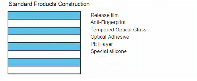
Phantom Glass is a brand of high-end tempered glass screen protectors designed for electronic devices like smartphones, tablets, and laptops.
It is the one of the toughest, strongest glass screen protection available in the market.
Key features include:
- High-strength protection: It can withstand heavy impacts, scratches, and daily wear and tear.
- Ultra-clear transparency: It’s almost invisible, maintaining the original clarity and color of your device’s screen.
- Fingerprint and smudge resistance: It has a special coating that makes it easier to clean and keeps the screen looking fresh.
- Easy installation: Typically designed for bubble-free application.
- Perfect fit: Custom-made for different brands and models of devices.
Best-in-Class Impact Resistance
9H Surface Hardness
Phantom Glass is manufactured with ion-exchange strengthened glass, offering superior durability against impacts, scratches, and surface wear.
In rigorous testing, Phantom Glass successfully passed 10 consecutive drops from a height of 1 meter directly onto the screen, meeting stringent standards required for aerospace-grade products.
Engineered for extreme resilience, Phantom Glass ensures maximum protection and structural integrity under the most demanding conditions.
In short, Phantom Glass is designed to protect your device screen as much as possible without affecting how it looks or feels.
Constructions and data:


E-paper/E-ink Front-light Introduction
LCD modules typically have a backlight because they are transmissive, but e-paper is reflective and does not have a backlight, making it perfectly usable in daylight. However, there is also a need for e-paper applications at night, which has led to the introduction of a new term, “front light” (前光). This also includes discussions on touch technology and lamination techniques associated with E-paper displays.
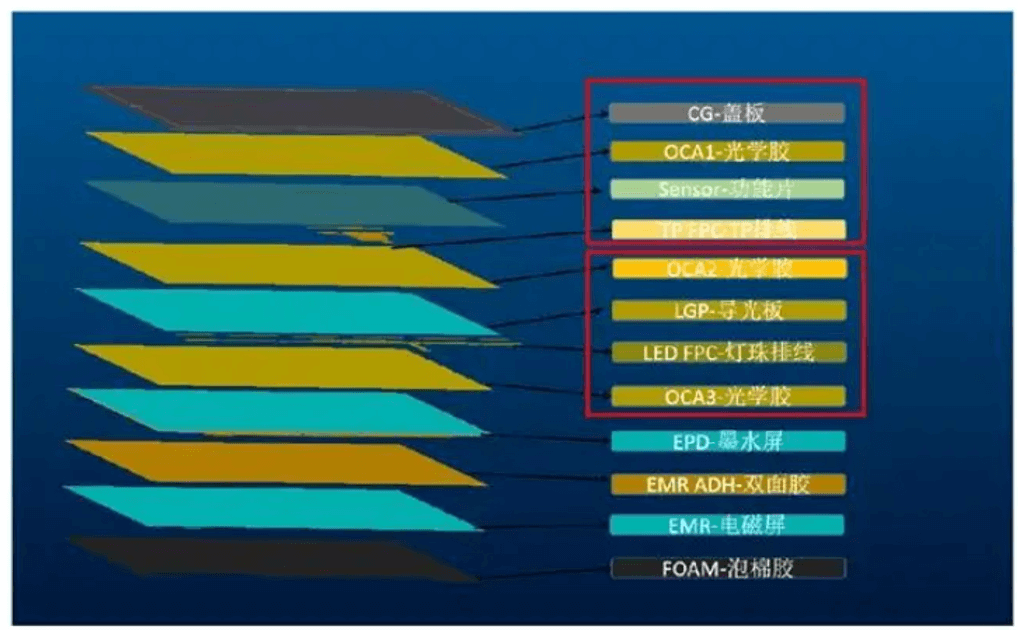
E-paper touch front light module structure
This is an overall diagram of the e-paper module. The upper red frame indicates the touch lamination, and the lower red frame shows the light guide component, followed by the EPD module and EMR. The touch lamination module consists of a cover plate, sensor, flexible circuit, and OCA. The front light component includes a light guide plate, OCA, and a flexible circuit containing beads. There are at least three layers of OCA, leading to a minimum of six lamination processes. The assembly plan is designed with one guide (dot pattern of the light guide plate), two types of lighting (cold and warm colors, or standard and high color gamut), three materials (materials for the light guide plate, sensor, and OCA), and at least six lamination processes.
Light guiding principle
This description refers to a schematic of a front light system, where light from a side-mounted source is manipulated using an input structure resembling gears and a dot pattern on the bottom. These structures refract or reflect the LED light, altering its direction to uniformly distribute it across the entire light guide plate. The illustration on the right shows this progression from a point (the light source) to a line (the light strip) to the entire surface of the light guide plate.
Color Saturation: Light Guide Plate Solution
Color e-paper modules, in comparison to monochrome ones, require light to pass through the RGB color filter twice, resulting in significant light loss, reduced brightness, and paler colors. To enhance brightness, changes were made to the dot patterns on the light guide plate. Smaller dots and adjusted angles increase effective light reflection. The angle of the dots was changed from 50° to 30°, which, through testing, increased light output by 10%.
Color Saturation: LED Bead Solution
Another approach to enhancing color saturation involves using LED lights. Specifically, using a blue LED chip that stimulates red and green phosphors to produce their respective colors. By enlarging the triangular areas where these interactions occur, the overall color gamut can be significantly broadened. In the images discussed, the left side exhibits some yellowish color distortion due to this effect. Despite all other aspects being the same, except for the type of LED beads, this results in markedly different visual outcomes.
The Impact of OCA Material
OCA material: The light guide plate has dots, typically concave. After lamination, the OCA fully immerses into the dots of the light guide plate, greatly impacting the optical matching and light guiding properties. The image on the left appears overall darker, which is also reflected in test data, whereas the data on the right shows overall brighter results. Just the difference in OCA materials can lead to this variation, hence the selection of different OCA materials is crucial for the corresponding product lamination.
The Impact of Sensor Material
Different sensor materials are currently used, mainly ITO Film and Metal Mesh. In terms of transparency, especially since color e-paper has higher demands for transparency, color e-paper generally prefers Metal Mesh. Both ITO Film and Metal Mesh work well with monochrome e-paper without any issues.
The Impact of Light Guide Materials
The material of the light guide plate significantly affects its performance because different materials influence the effectiveness of the dot patterns differently.
Should you have any questions about front-light, please contact our engineers.
Check out our E-paper products in stock here!
Introduction to E-paper
1. The Concept of E-paper
E-paper can maintain its display even when powered off, possessing a certain memory capacity and most functionalities of traditional paper. The base material of e-paper is primarily polyester compounds, coated with circuits on the surface. Changes in the external electric field control the movement of electronic capsules within the circuit to alter text and images. E-paper features low power consumption and flexibility, providing delicate display quality, a wide viewing angle, and excellent visibility under sunlight without any blind spots.
In 1999, E Ink Corporation first introduced a display using electronic ink. In 2007, Amazon released the first-generation Kindle e-reader, equipped with a 6-inch, 4-level e-ink display. From the classic black-and-white e-ink display to today, it has evolved to achieve full-color display capabilities with eight primary colors. Compared to traditional displays, e-ink screens have a bistable characteristic, meaning they only consume power when the pixel colors change. The screen can retain images even after the power is turned off. Moreover, as a display technology, e-ink screens can mimic the visual experience of printing and writing on paper.

2. Display Principles of E-paper
There are several technological approaches for e-paper, including Electrophoretic Display Technology (EPD), Cholesteric Liquid Crystal Display (Ch-LCD), Bistable Twisted Nematic Liquid Crystal Technology (Bi-TNLCD), Electro-Wetting Display Technology (EWD), Electrofluidic Display Technology (EFD), and Interferometric Modulator Technology (iMod). Among these, electrophoretic display technology is the most representative, having been in mass production for many years with mature processes, low cost, high performance, and closest resemblance to traditional paper.
Electrophoretic display technology is one of the earliest developed paper-like display technologies. Its basic principle involves using an external electric field to control the movement of charged particles within a liquid. When these particles move to a specific position, they display different colors.
Electrophoretic ink technology, commonly known as electronic ink, involves applying electronic ink onto a layer of plastic film, then overlaying it with a thin-film transistor (TFT) circuit. Controlled by a driving IC, this arrangement forms pixel graphics, creating Electronic Paper Displays (EPD). Unlike typical flat-panel displays that use light emission to produce images, electronic ink screens primarily employ electrophoretic display technology. They rely on reflecting ambient light for image display, making reading more comfortable. Moreover, the displayed images remain clear even under direct sunlight, with a very wide viewing angle, theoretically up to 180 degrees.
3. Construction of E-paper
Electronic Paper Displays (EPD) typically consist of anti-glare glass, a front light source, touch functionality, electronic ink film, a TFT backplane, a controller, and a power manager, among other components. The electronic ink film is usually composed of millions of microcapsules. These microcapsules contain black and white particles that are charged either positively or negatively. They move in response to changes in the electric field, allowing specific areas to appear black or white, thus forming the corresponding pixel graphics.


The core substance developed by E Ink Holdings for their microcapsule electronic ink technology is electronic ink, which mainly consists of two parts: black dye and white charged titanium dioxide electrophoretic particles.
The electronic particles are suspended in the dye, arranged uniformly and move randomly. They are encapsulated by a transparent shell. Under the influence of an external electric field, the white particles can sense the charge and move in different directions. The side where white particles accumulate can display white, while the opposite side shows the color of the dye, that is, black. E-paper uses this principle to achieve color transitions for text and images.

4. E-paper Materials
- Substrate Materials: E-paper substrates are typically made of plastic (such as polyester film) or glass. Plastic substrates have the advantage of being lightweight and flexible, making them suitable for creating bendable e-paper. Glass substrates, on the other hand, provide better protection and durability.
- Microcapsule Materials: Microcapsules are the core components of e-paper and are usually made of polymer materials. Each microcapsule contains black and white particles, which are typically made from materials such as carbon black or white titanium dioxide. The size of microcapsules generally ranges from a few microns to several tens of microns.
- Conductive Materials: The transparent electrodes of e-paper typically use indium tin oxide (ITO) or other conductive materials. These materials not only possess good conductivity but also high transparency, effectively conducting electricity without affecting the display quality.
- Ink Materials: The pigment particles used in electronic ink are usually made from inorganic or organic materials, offering good dispersibility and stability to ensure the clarity and longevity of displayed images.
- Protective Film: To enhance the durability of e-paper, a protective film is often applied to the surface. This film helps prevent scratches and external damage, thereby extending the lifespan of the e-paper.
5. E-paper Manufacturing Process
The technology of electrophoretic ink, commonly known as electronic ink, is central to the manufacturing process of e-paper. This process involves coating a layer of electronic ink onto a plastic film. A thin-film transistor (TFT) circuit is then laminated onto this coated film. Controlled by a driver IC, this arrangement facilitates the formation of pixel graphics, which are the building blocks of the Electronic Paper Displays (EPD). This method allows for precise control and manipulation of the ink particles within the microcapsules, enabling the display to show images and text by rearranging these particles under electrical influence.


To control production costs and considering the characteristics of electrophoretic display materials, current microcapsule electrophoretic display films are produced using a roll-to-roll coating method. This process allows for the rapid production of display materials that meet the requirements of product applications. The mentioned image would typically show the roll of film material as it is processed in this continuous manufacturing method.

6. Advantages and Disadvantages of E-paper
· Advantages
-
- Low Energy Consumption: E-paper consumes very low power, typically only using electricity when refreshing the display, thus using almost no power in standby mode.
- Good Readability: Due to its reflective display nature, e-paper maintains good readability under strong light, similar to that of traditional paper.
- Lightweight and Flexible: The lightness and flexibility of e-paper make it suitable for various portable devices and flexible displays.
- Eye Comfort: E-paper reduces glare and blue light radiation, making it more comfortable for long reading sessions.
· Disadvantages
-
- Cost: The production cost of e-paper is relatively high, which limits its proliferation in some low-end markets. However, the yield of electrophoretic display technology, especially microcapsule display technology, is expected to improve annually due to its simple manufacturing process and roll-to-roll coating method similar to paper production. As production volumes and yields increase, the cost of e-paper displays is expected to decrease annually. Like other electronics, the price of e-paper displays will likely continue to fall, leading to various emerging applications as costs decrease.
- Slow Refresh Rate: E-paper has a relatively slow refresh rate, making it unsuitable for displaying dynamic videos or rapidly changing content. To meet the performance requirements of bistability, e-paper display technology sacrifices response speed, with update times taking several hundred milliseconds, which is insufficient for video applications. With technological advancements, faster responding e-paper materials have emerged, and response times have been reduced to tens of milliseconds, with potential for further improvements to meet customer demands in the future.
- Full Colorization: Most e-paper display technologies are primarily monochrome, and color e-paper has higher costs and technical challenges. Currently, color electrophoretic display e-paper can be achieved in two ways: one using a color filter over black and white e-paper, and the other using colored particles or dyes, with samples already produced. However, because it relies on reflected light for imaging, e-paper screens appear somewhat dim compared to the brightness and color accuracy of LCD screens. Thus, colorization is a revolutionary breakthrough for e-paper technology, with significant resources being devoted to research and development, promising the future availability of color e-paper displays.
- Durability: While e-paper is relatively durable, its performance may be impacted under extreme conditions (such as high temperatures and humidity). Unlike conventional readers who might not expect to roll up a book, the primary purpose of using flexible e-paper displays is not to be rollable but to be portable and impact-resistant. Flexible e-paper displays can opt for plastic substrates as backplanes. E-paper with plastic substrates is about 80% lighter than those made with glass materials and only about 0.3 mm thick, meeting the demands for lightweight, thin, and impact-resistant features. However, the biggest challenge for plastic substrates is their heat resistance and chemical stability, requiring ongoing improvements in substrate materials.
7. Applications of E-paper
- E-book Readers: E-paper is most famously used in e-book readers, such as Amazon’s Kindle. Due to its paper-like reading experience, e-paper allows users to read for long periods without significant eye fatigue.

- Billboards and Information Displays: Many businesses and public spaces are beginning to use e-paper for billboards and information display systems. E-paper’s clarity in sunlight and low energy consumption make it ideal for displaying information over extended periods.

- Smart Labels: In retail and logistics, e-paper labels (such as electronic shelf labels) are widely used. They can be updated in real-time with price and product information, reducing the costs associated with manual updates.

- Wearable Devices: Some smartwatches and fitness trackers have started incorporating e-paper display technology to enhance battery life and improve readability under various lighting conditions.

- Educational Devices: E-paper technology is gradually being adopted in the education sector, for example in electronic exam papers and learning tablets, offering a more flexible and environmentally friendly way of learning.
Check out our E-paper products in stock here!
Core board to Baseboard Connection
The physical methods of connecting a core board to a baseboard depend on design requirements, cost, reliability, and the manufacturing process. Below are some common connection methods:
1. Socket Connectors:
- Utilizing board-to-board connectors, this is a very common method of connection. By using socket connectors, the core board can be inserted into a corresponding socket pre-installed on the baseboard. This type of connection is typically used in applications where the core board needs to be frequently replaced or upgraded, such as interfaces between computer motherboards and CPUs.


2. Direct Soldering:
- The pins or solder pads of the core board can be directly soldered onto the baseboard. This method provides a very stable and reliable connection, suitable for permanent installations where disassembly is not required, such as in certain embedded system applications.
- DIP (Dual In-line Package) Insertion: This refers to a specific type of direct soldering where components with DIP packaging are inserted into through-holes on the baseboard and then soldered.

- Stamp Hole Technique:
-
- In this method, two boards are connected at their edges by a small strip of material featuring many tiny holes, facilitating easy breakage. After breaking, the edges of the boards resemble the perforated edges of a postage stamp, hence the name “stamp hole” for this type of paneling.
- As demand for modular circuit boards increases in printed circuit board manufacturing, the use of finer holes (also known as stamp holes) is becoming more common. For irregularly shaped PCBs, such as circular ones, stamp holes are used to facilitate panel connections, making them particularly useful in non-standard board designs.
- In terms of stability, the stamp hole design is considered optimal. While DIP pins and board-to-board connectors present challenges in wiring and soldering, and though board-to-board connectors can use surface-mounted imported interfaces, they are expensive and prone to poor contact after multiple insertions and removals. Stamp holes, on the other hand, offer low cost, ease of wiring, stability, and firm soldering with a low profile, making them the best choice for products requiring high shock resistance. However, stamp holes also present some difficulties, such as the challenge in testing to verify the integrity of the core board, and the risk that once soldered, it is difficult to remove without risking damage to both the core board and the baseboard.


3. Slots and Edge Connectors, or Gold Fingers:
- The core board can be designed with edge connectors, which can be inserted into corresponding slots on the baseboard. This method is commonly used in PC components such as RAM sticks and graphics cards and is also suitable for some high-performance embedded systems. Edge connectors provide a reliable and quick method for assembling and disassembling components, facilitating upgrades and maintenance.

4. Screw Mounting or Standoffs:
- Screws are used to directly secure the core board to the baseboard. This method enhances physical stability, making it suitable for environments subject to vibration or other applications requiring additional mechanical fixation. Standoffs provide the necessary spacing and support to maintain board integrity and prevent electrical shorts, ensuring durable and reliable installations.


5. Backplane and Motherboard:
- In some large systems, multiple core boards or modules can be connected via a backplane, which in turn is connected to the main motherboard. This arrangement supports the high-density installation of core boards and is commonly found in servers and telecommunications equipment. The use of a backplane allows for centralized connectivity and power distribution, facilitating easier upgrades and maintenance while optimizing the performance and scalability of the system.

6. Flexible Flat Cables (FFC) or Ribbon Cables:
- Core boards and baseboards are connected using flexible cables, which provide a degree of physical positioning flexibility. This method is particularly suitable for devices with limited space or complex wiring requirements. Flexible flat cables and ribbon cables facilitate easier routing and connection in tight or intricate layouts, reducing the risk of damage during installation and maintenance while ensuring reliable signal transmission.


Each connection method has its specific applications, advantages, and disadvantages, and the choice of the appropriate method depends on the specific needs and budget of the project. If you have a particular project or design considerations, we can further discuss the most suitable connection solution.
LCD Display ESD Standards and Improvement
IEC 61000-4-2 is an electromagnetic compatibility (EMC) standard developed by the International Electrotechnical Commission (IEC), specifically aimed at testing the immunity to electrostatic discharge (ESD). This standard is designed to evaluate and verify the ability of electronic equipment and systems to withstand electrostatic discharge. It defines the procedures for electrostatic discharge testing and various testing levels.
1. IEC 61000-4-2 Testing Levels
The IEC 61000-4-2 standard defines two main types of discharges:
1) Contact Discharge: Electrostatic discharge is directly applied to the device through a test electrode in contact with it.
Air Discharge: Electrostatic discharge is applied by bringing the test electrode close to the device (without direct contact).
Each type of discharge has different voltage test levels to simulate the intensity of electrostatic discharge that might be encountered in various environments. The standard test levels defined in IEC 61000-4-2 are as follows:
Contact Discharge Levels:
- Level 1: 2 kV
- Level 2: 4 kV
- Level 3: 6 kV
- Level 4: 8 kV
- Special Level: > 8 kV (Higher voltage levels can be defined by the user based on actual needs)
Air Discharge Levels:
- Level 1: 2 kV
- Level 2: 4 kV
- Level 3: 8 kV
- Level 4: 15 kV
- Special Level: > 15 kV (Similarly, higher voltage levels can be defined by the user based on actual needs)
For LCD Display only, the maximum testing is Level 4.
2. Test Procedure
During the actual testing process, the equipment must undergo a series of prescribed electrostatic discharge operations to ensure it can withstand the expected electrostatic discharge environment. The specific testing procedure includes:
1) Selecting the Test Level: Choose the appropriate test level (Level 1 to Level 4, or a higher special level) based on the expected usage environment of the equipment.
2) Setting Up the Test Equipment: Use an electrostatic discharge gun and other necessary testing equipment as specified by the IEC 61000-4-2 standard.
3) Discharge Methods:
- Contact Discharge: Directly contact the tip of the discharge gun with the metal parts of the equipment.
- Air Discharge: Bring the tip of the discharge gun close to the non-metallic parts of the equipment, gradually approaching until a discharge occurs.
4) Repeating the Discharge: Typically, multiple discharges (usually 10 or more) are required at each test point to verify the equipment’s electrostatic discharge immunity across all test points.
5) Observation and Recording: After each discharge, observe the equipment’s response (such as reboot, data loss, function failure, etc.) and record the test results.
3. Main Phenomena of LCD Screen ESD Test Failures
When an LCD screen fails an ESD (Electrostatic Discharge) test, the following phenomena are commonly observed:
1) Screen Flickering or Blinking: The display may flicker or blink intermittently due to instability caused by electrostatic discharge.
2) Permanent Display Artifacts: Permanent lines, spots, or distortions may appear on the screen, indicating damage to the LCD panel or circuitry.
3) Screen Freezing: The display may freeze or become unresponsive, requiring a reboot or power cycle to recover.
4) Color Distortion: Colors on the screen may become distorted or incorrect, which could be due to damage to the display driver or other electronic components.
5) Loss of Display Functionality: The screen may go completely blank or fail to display any image, suggesting a more severe failure of the screen’s internal components.
6) Touch Function Malfunction (if applicable): In touch-enabled LCD screens, the touch function may become unresponsive or erratic after an ESD event.
7) Unexpected Reboots: The device might reboot unexpectedly due to the ESD affecting the device’s power management or control circuits.
8) Data Loss or Corruption: There may be a loss or corruption of data, particularly if the ESD affects the memory or storage components.
These phenomena indicate that the LCD screen or its associated electronics have been compromised by electrostatic discharge, requiring further investigation and potentially additional shielding or circuit protection.
4. Electrostatic Discharge (ESD) Improvement Measures
1) Preventive Measures During the Design Phase
a. Board-Level Design
- Ground Plane Design: Ensure that the PCB has a complete ground plane to enhance its resistance to interference. A solid ground plane helps in providing a low-impedance path for current flow, effectively reducing noise and improving the overall electromagnetic compatibility (EMC) of the board.
- ESD Protection Devices: Add ESD protection devices on critical signal lines, such as TVS (Transient Voltage Suppression) diodes and ESD protection capacitors. These components help to clamp voltage spikes and safely dissipate ESD energy, protecting sensitive circuits from damage.
- Signal Return Path Optimization: Optimize the signal return paths to minimize the ESD current passing through critical circuits. Properly designed return paths ensure that the ESD currents are directed away from sensitive areas, reducing the potential for circuit damage and improving overall ESD resilience.
b. Enclosure Design
- Conductive Coating: Apply a conductive coating on the inside of plastic enclosures to provide a shielding effect. This coating helps to block and dissipate electrostatic discharge (ESD), protecting the internal components.
- Grounding of Metal Enclosure: Ensure that the metal enclosure is properly grounded to provide an effective path for ESD discharge. Good grounding helps in safely dissipating static electricity away from sensitive electronics.
- Increase Grounding Area Between TFT LCD Metal Frame and Product PCB: Expand the grounding area between the metal frame of the TFT LCD and the product’s PCB. This helps to create a more effective ESD path and improves overall device immunity to electrostatic discharges.
- Increase Floating Gap Between Enclosure and TFT Touch Screen: Increase the floating gap between the enclosure and the TFT touch screen. A larger gap can help to minimize the direct impact of ESD on the touch screen by providing more space for potential discharge to dissipate without affecting the sensitive components.
2) Wiring and Layout Optimization
- Protection of Critical Components: Place sensitive components away from areas that are likely to come into contact with ESD, such as buttons, connectors, and interfaces. This reduces the risk of ESD reaching these components and causing damage.
- Short Grounding Wires: Minimize the length of grounding wires to reduce ground resistance and inductance. Shorter grounding paths provide a more efficient route for ESD currents to dissipate, improving overall protection.
- Isolation Zones: Create dedicated ESD protection zones on the PCB to isolate sensitive circuits from areas that might come into contact with ESD. This can involve adding barriers, grounding planes, or guard traces to shield critical components from potential discharge paths.
3) Filtering and Buffering
- Filtering Capacitors: Add filtering capacitors to critical signal lines to absorb ESD pulses.
- Series Resistors: Place small resistors in series with signal lines to limit ESD current.
4) Filtering and Buffering
- Filtering Capacitors: Add filtering capacitors on critical signal lines to absorb ESD pulses.
- Series Resistors: Place small resistors in series with signal lines to limit ESD current.
5) Shielding and Grounding
- Shielding Covers: Install metal or ITO (Indium Tin Oxide) shielding covers on LCD monitors to reduce the direct impact of ESD.
- Grounding Path Optimization: Ensure that shielding covers, conductive coatings, and metal enclosures have good grounding connections to form a low-impedance ESD discharge path.
6) Interface and Button Protection
- Interface Protection: Add ESD protection devices, such as TVS diodes, at the input and output interfaces of the display.
- Button Protection: Design proper shielding and grounding for buttons to reduce ESD interference conducted through them.
7) Power and Ground Line Handling
- Isolation Transformers: Use isolation transformers to separate the power section from the signal section, reducing the possibility of ESD conduction through the power supply.
- Ground Line Handling: Add common mode chokes and filtering capacitors at the power input to reduce the possibility of ESD conduction through power lines.
8) Product Testing and Validation
- ESD Gun Testing: Use an ESD gun for simulated testing to identify weak points and implement corrective measures.
- Repeated Validation: Conduct repeated ESD tests in different environments to ensure that corrective measures are effective.
9) Material Selection
- Antistatic Materials: Choose materials with antistatic properties for the monitor enclosure, such as antistatic plastics.
- Conductive Rubber: Use conductive rubber at buttons and interfaces to enhance antistatic capability.
5. Specific Improvement Examples
1) SD Protection for Monitor Interfaces
To protect the HDMI, VGA, USB, and other interfaces on a monitor from ESD (Electrostatic Discharge), consider the following protection strategies:
- Parallel TVS Diodes: Install Transient Voltage Suppression (TVS) diodes in parallel on the signal lines of HDMI, VGA, USB, and other interfaces. TVS diodes help clamp voltage spikes caused by ESD, protecting sensitive circuitry from high-voltage surges.
- Adding Small Capacitors: Place small capacitors near the interfaces to form low-pass filters. These capacitors help to absorb and filter out high-frequency ESD pulses, further protecting the internal components of the monitor.


2) ESD Protection for Buttons
To protect buttons from electrostatic discharge (ESD), the following measures can be implemented:
- Conductive Rubber Pads: Place conductive rubber pads between the buttons and the circuit board to ensure effective grounding when the buttons are pressed. The conductive rubber provides a path for ESD to dissipate safely to the ground, reducing the risk of damage to the circuit.
- Series Resistors: Insert small resistors in series with the button lines. These resistors help limit the ESD current that might flow into the circuit, providing additional protection for sensitive components by reducing the impact of ESD pulses.
3) ESD Protection for Power Lines
To protect against electrostatic discharge (ESD) through the power lines, the following measures can be used:
- Common Mode Chokes: Install common mode chokes at the power input. These chokes help suppress common-mode noise and reduce the amount of ESD energy that can be conducted through the power lines.
- X/Y Capacitors: Use X and Y capacitors at the power input to filter out ESD pulses conducted through the power lines. X capacitors are placed across the line and neutral, while Y capacitors are connected between the line/neutral and ground. Together, they form an effective filtering network to absorb and mitigate high-frequency ESD pulses.
4) Reset Pin with RC Circui
To protect the reset pin from ESD and ensure stable operation, an RC (Resistor-Capacitor) circuit can be added. The suggested values for the components are:
- R1 = 1 kΩ (1 kilo-ohm): This resistor helps to limit the current flowing to the reset pin, providing a buffer against sudden voltage spikes due to ESD.
- C1 = 0.1 µF (microfarad): This capacitor acts as a filter, smoothing out any rapid voltage changes and providing stability to the reset signal.
- C2 = 0.047 µF (microfarad): An additional capacitor can be placed in parallel to further refine the filtering, ensuring the reset pin is less susceptible to high-frequency noise and ESD pulses.
This RC circuit helps to debounce the reset pin and provides added protection against electrostatic discharge and transient voltage fluctuations.

5) Adding an ESD Ring
It is recommended to add TVS ESD protection devices at electrostatic contact points to take advantage of their antistatic properties, forming an ESD discharge path and enhancing protection. Additionally, include an electrostatic discharge ring (ESD ring) on the panel. This ring provides a path to ground for electrostatic discharge, thereby protecting the VCOM and Gate lines from potential damage.

6) Add a TVS at Each VCOM Point
It is recommended to add a TVS (Transient Voltage Suppression) diode at each VCOM point for enhanced ESD protection. Specifically, use the ULC0511CDN in a DFN1006 package from LeiMao Electronics. This component has been successfully applied and has shown satisfactory results among many display customers.

7) Exposed Traces on the Panel
Apply insulating glue or tape over any exposed traces on the panel. This helps to prevent accidental short circuits and protects the traces from ESD damage.
8) Unused Pins
Unused pins should not be left floating; instead, they should be connected to MVDDL (minimum voltage differential digital logic). This prevents floating pins from picking up noise or causing unintended behavior in the circuit.
9) Software Reset
Implement a software reset function. This allows the system to recover from unexpected conditions or malfunctions due to ESD events or other issues by resetting the software to a known good state.

10) Example: Automotive LCD Display Screen
Problem Description: During electrostatic discharge (ESD) testing, the screen passed at ±6 kV contact discharge but failed at ±8 kV air discharge.
Analysis: The LCD screen is connected to the main controller via wires, and the interface type used is LVDS (Low-Voltage Differential Signaling). Currently, large screens primarily use LVDS and VBO (Video Bus Output) differential interfaces, which are effective at suppressing common-mode interference. The screen flickering observed during testing may be caused by interference affecting the LVDS cables. Contact discharge of 500V-1000V was applied to each signal line of the LVDS cables, and it was found that screen flickering occurred at 500V-1000V on both pairs of differential clock lines. This confirmed that the differential clock signals are particularly susceptible to ESD interference.
Solution: Add ferrite beads (magnetic rings) to the LVDS lines. After adding the magnetic rings, the ESD tests were conducted again, and the tests passed successfully. The chosen ferrite bead has the following frequency impedance characteristic curve:
[Include the frequency impedance characteristic curve of the ferrite bead here if available in a visual format.]
By implementing these ferrite beads, the susceptibility to ESD interference was significantly reduced, stabilizing the differential clock signals and preventing screen flickering.

11) Antistatic Methods for Different Enclosures
TFT LCD displays are easily affected by electromagnetic interference (EMI) and electrostatic discharge (ESD), especially when they have built-in touchscreens. Regarding ESD, TFT LCD displays are mounted flush on the exterior of the device. Discharges can reach the edges of the LCD frame and are not completely dissipated by the product enclosure.

Looking at it in more detail, the frame of an LCD screen is usually connected to the signal ground (GND) of the product’s PCB. Therefore, any discharged current can flow into the device’s board. The solution depends on whether the final product’s enclosure is conductive or non-conductive.
- Conductive (Metal) Enclosure: Ensure tight electrical bonding on all surfaces between the LCD frame and the edges of the bezel step. Use a transparent conductive coating, such as ITO (Indium Tin Oxide), with surface resistivity extending to the edges of the bezel step.
- Non-Conductive Enclosure: Provide the TFT LCD display as an entry point for ESD. Use shielded flat cables to connect the LCD frame to the PCB ground; increase the insulation gap (floating) between the product enclosure and the LCD display module.
12) Example: White Screen/Blue Screen Issue
A “white screen” or “blue screen” refers to the module’s screen displaying only the backlight, as it does when initially powered on, without any response even when adjusting the contrast.
This issue occurs because interference is applied to the module’s power supply lines (VDD or VSS) or to the RESET signal line during operation, causing the module to reset. The reset results in the initialization of the module’s internal registers and turns off the display.
Solution:
- If the interference is on the power supply lines, it is recommended to add a decoupling capacitor (10 µF) and a filtering capacitor (0.1 µF/0.01 µF) between the VDD and VSS power lines as close to the module as possible.
- If the interference is on the RESET signal line, it is advisable to add a filtering capacitor (with a capacitance of 0.1 µF or 0.01 µF) between the RESET signal line and VSS as close to the module as possible.
The choice of capacitor values should be determined based on the actual test results.
13) Display Shows Incorrect Characters or Random Pixels (Data Errors) That Can Only Be Resolved by Power Cycling
This issue occurs because interference is applied to the control signals, causing the register parameters to be modified. Typically, when displaying data, there is no repeated writing to the main working register parameters, leading to the described issue.
Solution:
If interference is present on the transmission lines:
- Use ferrite beads, or shield the lines with materials like tin foil or thin copper sheets.
- Change the routing of the transmission lines to avoid areas with interference.
- Shorten the length of the transmission lines or add line drivers to increase drive strength and improve noise immunity.
14) What to Do If Interference Points Cannot Be Found or Circuit Precautions Are Insufficient to Eliminate Interference?
If interference cannot be identified or circuit precautions fail to prevent its impact, consider the following solutions:
Periodic Register Initialization: Instead of using the RESET signal, perform operations directly on the registers for initialization. If a crash occurs and cannot be recovered, use the RESET signal for initialization. However, this may cause screen flickering during normal display. To ensure normal display is not affected by initialization:
a. Use Register Read Data for Initialization: Use data read from registers, such as reading display status words or specific SRAM unit data, as the basis for determining whether initialization is needed.
b. Use Negative Display Module with Backlight Control: For modules with a negative display, turn off the backlight when not in use, making it difficult to see the display content. When the display content needs to be observed, turn on the backlight, using this moment as the point to reinitialize the module, which is less noticeable.
15) Electrostatic Interference Testing on Product Enclosure (Especially Product Panel) Causes White Screen or Display Errors on the Module
This type of interference is mostly caused by the module’s metal frame or glass interfering with the module’s circuitry. To improve this situation, consider the following methods:
- Connect the module’s metal frame to ground.
- Connect the module’s metal frame to VSS (ground of the circuit).
- Leave the module’s metal frame floating (not connected to anything).
- Add an insulating pad between the module’s metal frame and the metal enclosure; the thicker the insulating pad, the greater the reduction of static electricity.
These four methods should be tested in the actual product to determine which one is most effective.
16) White Screen or Display Errors Occur Even Without External Interference Source
This situation also falls under interference, but it is due to internal system interference, mainly caused by software conflicts. The first step is to identify the pattern of when the interference occurs. Such issues are more likely to happen during the module’s write process, leading to the module freezing or displaying errors.
Common causes include:
- Interrupt routines interfering during module operations (I/O addressing mode), leading to incorrect operations such as modified control signals or data, which can cause the module to freeze or display incorrectly.
Solution: Disable interrupt responses while operating the module to prevent interference during critical processes.
17) Example: When using a TFT display and a product chassis made of metal, an 8000V electrostatic discharge (ESD) test was conducted, which caused the display to show a garbled screen. Resetting and reinitializing the module had no effect, and the device had to be powered off and restarted to return to normal operation. Industry regulations do not allow grounding of the chassis.
As a solution, the metal chassis was replaced with an acrylic (organic glass) enclosure, and a timed loop refresh (initialization) program was added to the main software routine. During the ESD test, when the LCD module is reset due to static discharge, the refresh (initialization) program corrects the issue, causing only a brief flicker before returning to normal operation, thus passing the test.
18) Example: Using a TFT display, an 8kV electrostatic discharge (ESD) test was conducted on the product chassis, resulting in the module showing no display
To improve this, a 330μF capacitor and a surge protection diode (P6K1) were added to the power pin of the module, and a 330μF capacitor was added to the output (VOUT) of the driver power supply. These measures significantly improved the situation. Additionally, the module’s metal frame was insulated from the chassis, maintaining a 2mm gap, which helped pass the ESD test.
However, despite these improvements, there were still occasional instances of no display. To fully resolve this, a periodic initialization routine was added to the program to reset the module and recover from interference. This completely solved the display interference issue.
19) Example: When using a TFT display, during a test where a 4kV, 150Hz positive pulse group interference signal was applied to the system’s main power line, the display showed garbled characters
To address this issue, a surge absorber was added to the power line at the LCD module interface, and the length of redundant transmission lines was reduced. These measures allowed the system to pass the test.
20) When using a TFT display on a switchgear cabinet, the module showed no display under high-voltage electromagnetic interference
To resolve this issue, the system power supply was replaced with an isolated power supply. A 0.01μF capacitor was connected to the /RESET pin of the module, the jumper connecting the module’s metal frame to VSS was disconnected, and an insulating pad was added to isolate the module’s metal frame from the switchgear cabinet.
21) The connection cable between the TFT display and the system motherboard is over 700mm long. When repeatedly writing graphic data, the right side of the graphic progressively duplicates the rightmost byte of graphic data
Measurements of the input signal waveform at the module interface were good, with /WR = 0 width of 2μs. Adding capacitors and pull-up resistors to the interface signals showed no significant improvement. Shortening the cable and adding ferrite beads provided noticeable improvement, but did not completely solve the issue.
Inserting a Schmitt trigger circuit (74HC14) into the /WR signal line completely resolved the problem. Additionally, inserting a 680Ω resistor into the /WR signal line also achieved a complete fix.
22) Example: Blue Screen on LCD Display
During ESD (Electrostatic Discharge) testing, an industrial display experienced blue screens every time the system was tested at ±6kV on the network port, USB, and serial port, causing the system to crash. It would recover automatically after power cycling, but the test was not passed. The board had previously undergone multiple design revisions focusing on grounding, filtering, and isolation, but these did not resolve the issue. Therefore, this time, a strategy was adopted to diagnose and rectify the root cause to identify and address the system’s weaknesses.
Analysis and Solution:
Based on the observed phenomenon, it was suspected that the CPU functional unit was being affected by interference. The core sub-board (CPU module circuit) pins were analyzed, and signals were identified as being particularly sensitive and prone to ESD interference based on practical experience and signal functionality.
To identify ESD-sensitive signals, an ESD gun was used to apply contact discharge at voltages of 100V, 300V, 600V, and 1000V to various signal pins on the core sub-board. During these tests, the problem did not reoccur, ruling out those signals as the source of the issue.
Further analysis of sensitive circuits on the core sub-board revealed that when a 100V contact discharge was applied to the sensitive DDR_CLK signal, the problem consistently reoccurred. Each time the discharge was applied, the issue was replicated. The DDR_CLK trace was 4 mils wide, and the design did not include test pads, limiting available mitigation options.
To determine if the static electromagnetic field was affecting the DDR_CLK clock signal, a grounded metal wire was placed directly above the DDR_CLK trace, and the ESD gun was used to discharge at the ground wire’s copper lug at 6kV. The issue was reproduced within five discharges, confirming that the electromagnetic radiation from the ESD was impacting the DDR_CLK signal and DDR components.
Resolution:
After confirming that the electromagnetic radiation was affecting the DDR module on the core board and causing the ESD issue to recur, a copper foil was used to shield and ground the core board area, protecting the sensitive DDR signals and module. After shielding the core board module, contact discharges were applied to the IO interfaces at ±6kV, 8kV, and 10kV, with each test involving 40 consecutive discharges. The system continued to operate normally, indicating that the issue was resolved.
Cause Analysis:
Further verification determined that the ESD affecting the entire system was due to radiative coupling or capacitive coupling. Analysis showed that the electrostatic discharge path was as follows: IO interface → single board PGND → metal backing plate → metal chassis → chassis cover → ground wire.
This path explains how the ESD was able to impact the sensitive components, confirming the need for additional shielding and grounding to protect against interference.

When the chassis cover is not screwed onto the metal chassis or when the cover is not in place, it was observed that there were no issues with electrostatic discharge (ESD). This ruled out the problem of radiative coupling. In this case, the ESD discharge path is as follows: IO interface → single board PGND → metal backing plate → metal chassis. This suggests that there is electrostatic capacitive coupling between the sensitive DDR area on the core board and the chassis cover (as they are very close to each other), as shown in the diagram below.

In summary, a simplified model of the electrostatic coupling on the core sub-board of the entire system is shown in the diagram below:


When diagnosing the issue, after adding a shielding cover to the core sub-board, the electrostatic coupling model at this point is shown in the diagram below.
From the diagram, it can be seen that after adding a shielding cover to the core sub-board, the electrostatic energy from the chassis back cover is directly coupled to the metal shield. This energy is then discharged to the ground through the shielding cover’s grounding pins, thereby preventing ESD from directly coupling into the DDR-sensitive module and resolving the issue.
Based on the above analysis, the ESD problem was caused by capacitive coupling of electrostatic interference from the chassis back cover to the DDR module circuit.
Since the core sub-board is a platform product of the client company and the DDR circuitry on the module is highly sensitive, it is recommended to use a shielding cover to protect the sensitive core sub-board module for both testing and mass production. This solution is simple, effective, and reliable.

23) EMI Protection for LCD Displays
The main approach is to shield components that are easily affected by EMI.
a. For sensitive components such as the Touch controller and LCD driver IC, use EMI shielding fabric to provide single-sided or double-sided protection.
b. Since some LCD screens emit high-frequency signals, shielding can be applied using a metal frame on the bottom and an ITO (Indium Tin Oxide) layer on the top.