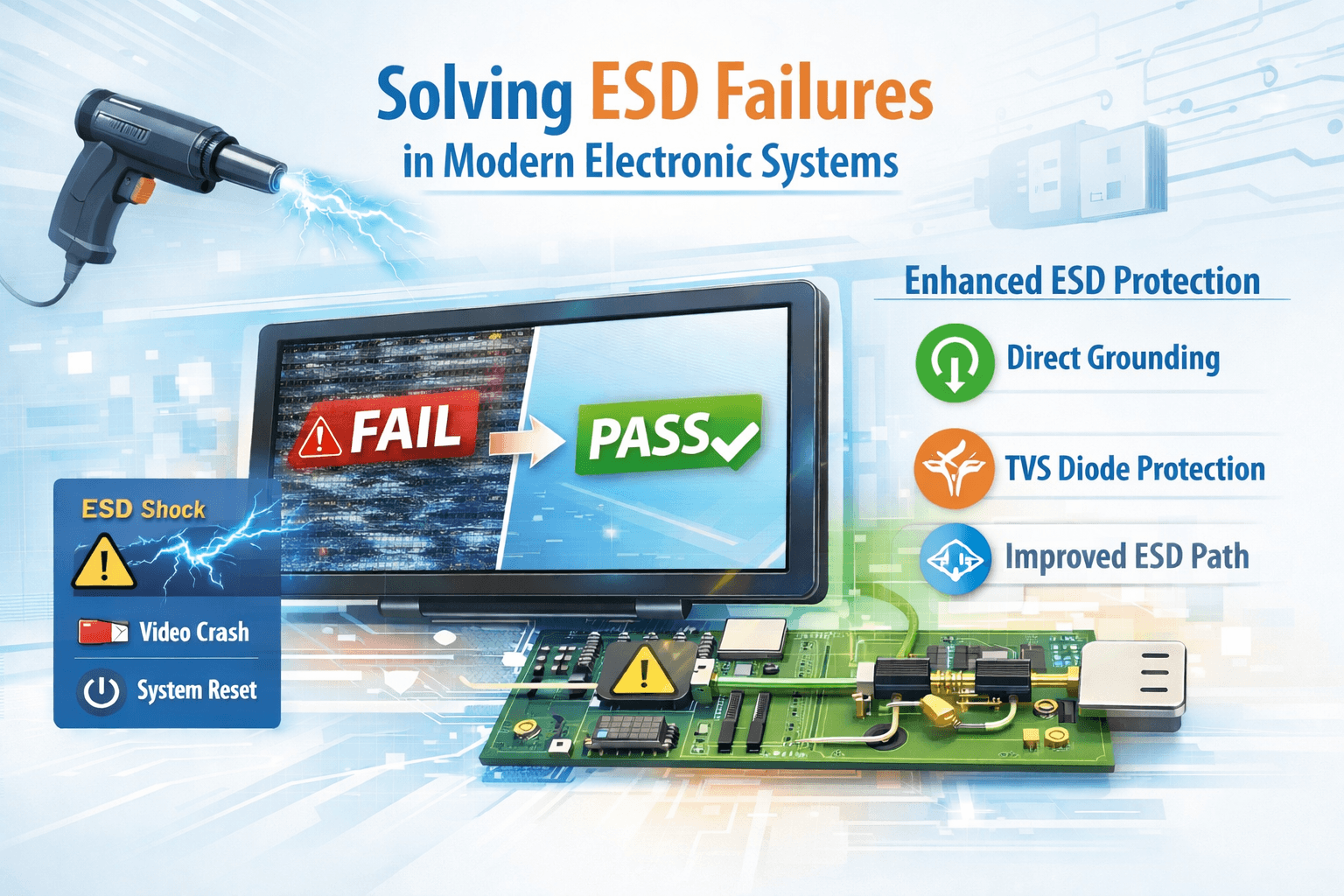
Case Overview – Improving ESD Reliability in large size USB Display System
The exiting display system was upgraded from an older LVDS design to a new USB‑based architecture. During certification testing, the system passed the 8 kV contact discharge test but failed the 15 kV air discharge test. This caused video interruptions and system resets, preventing the product from being approved.
Our engineering team analyzed the issue and identified two main causes:
- The USB ground path had too much resistance during an ESD event.
- The USB power line did not have strong enough protection against voltage spikes.
After making targeted improvements, the system able to successfully pass the 15 kV air discharge test.
What Was Happening?
During testing, an ESD gun applies a high‑voltage static shock to the outside of the device. This simulates real‑world situations such as a user touching the screen after walking on carpet.
This shock caused the USB interface to momentarily fail, which led to:
- Video freezing
- Display blackouts
- Touch panel communication loss
- System resets
This happened because the USB interface is more sensitive to static electricity than the older LVDS design.
Root Cause Debug
-
Grounding Was Too Weak for ESD
The USB ports used ferrite beads between the connector and ground. Ferrite beads are good for filtering noise, but they block fast, high‑energy ESD pulses. This prevented the static charge from safely going to ground.
-
The USB Power Line Needed Better Protection
The USB 5 V line did not have a fast‑acting protection device to absorb sudden voltage spikes caused by ESD.
What We Changed
To fix the issue, we made four improvements:
✔ Direct Grounding
We removed the ferrite beads (L15 and L20) and connected the USB ground directly to the system ground.
This gives static electricity a clean, low‑resistance path to escape.
✔ Added TVS Protection
We added a high‑speed TVS diode (SP1326‑01LTG) to the USB 5 V line.
This device instantly clamps voltage spikes and protects the USB controller.
✔ Improved ESD Path
The new grounding and protection layout ensures that ESD energy is safely diverted away from sensitive components.
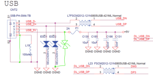
Figure 1
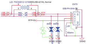
Figure 2
How the Improved Design Works
Before Fix
ESD Shock → Ferrite Bead → Blocked → USB Chip Overloaded → Video Failure
After Fix
ESD Shock → Direct Ground → TVS Clamp → USB Chip Protected → System Stable
Results
After applying these improvements:
- The system passed 15 kV air discharge
- No video dropouts or resets occurred
- USB communication remained stable
- The product is now ready for certification, BINGO!!
Conclusion
The ESD failures were caused by grounding impedance and insufficient surge protection in the USB interface. By optimizing the ground path and adding proper TVS protection, we restored the system’s reliability and ensured it meets certification requirements.
If you have any questions, please contact our engineering.