Blog
A Complete Guide to the Functions of Common Driving Voltages in TFT-LCD Display Modules
We will explain several common driving voltages in a TFT-LCD module from an engineer’s perspective: what each voltage rail does, the typical voltage ranges, which components use them, and what needs attention during design.
What voltage rails are present in a TFT-LCD module
Typical small- to medium-size TFT-LCD modules commonly include the following voltage rails:
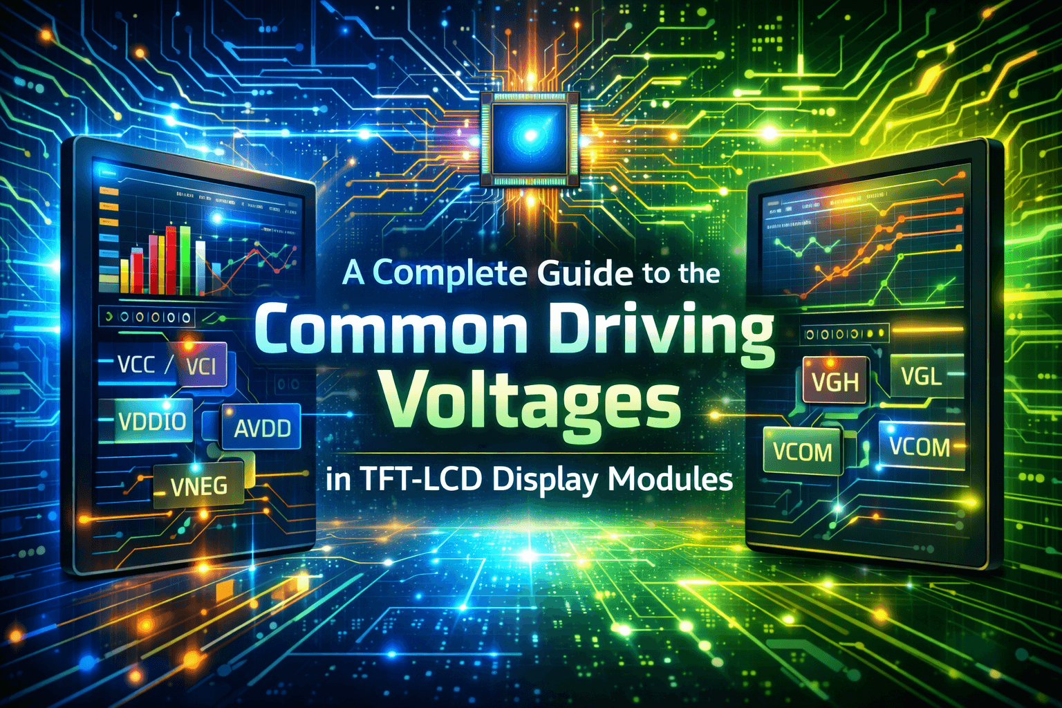
- VCC / VCI: Digital core power supply (MCU/interface logic)
- VDDIO: I/O power supply (pixel data/control signal interfaces)
- AVDD (or the positive rail in VPOS/VNEG): Analog power supply for the source driver IC and the upper limit of the pixel voltage range
- VNEG (sometimes called VNS, VGLS, etc.): Negative power supply for the source driver and the lower limit of the pixel voltage range
- VGH: Gate high voltage, the TFT gate “ON” voltage
- VGL (or VEE, GVEE, etc.): Gate low voltage, the TFT gate “OFF” voltage, typically a negative voltage
- VCOM: Common electrode reference voltage (Common Electrode), which determines the center point of the liquid crystal’s alternating drive
Many dedicated PMICs (such as TPS65156, for example) are designed specifically to convert a single 3.3–5 V input into the multiple voltage rails above for TFT-LCD panels and their driver ICs.
VCC / VCI / VDDIO: Digital Logic and Interface Power
Function
- Supplies power to the internal digital circuits of the LCD driver IC, timing logic, and interface controller (such as RGB/8080/SPI interface logic).
- Powers the I/O buffers connected to the main controller SoC (e.g., VDDIO), ensuring voltage-level compatibility such as 3.3 V or 1.8 V.
Typical Range
- VCC / VCI: Generally 2.5–3.3 V; some driver ICs support down to 1.8 V.
- VDDIO: Common values are 1.8 V / 2.8 V / 3.3 V, matching the I/O voltage of the host controller.
Engineering Considerations
- Power-up sequence: Digital power and logic levels usually need to stabilize before or at the same time as analog voltages such as AVDD and VGH/VGL, to prevent the driver IC from entering an abnormal state (see the specific IC datasheet for details).
- Signal level matching: The I/O voltage of the main controller must match the module’s VDDIO; otherwise, level shifting is required.
AVDD / VPOS / VNEG: Source Driver Analog Power and Pixel Voltage Range
Function
- AVDD (or the VPOS/VNEG pair) is the power supply rail for the analog output of the source driver, used to store a voltage corresponding to each pixel’s grayscale level.
- The source driver outputs different voltage levels between AVDD and VNEG to each subpixel capacitor, thereby changing the voltage difference across the liquid crystal and adjusting light transmission.
Typical Range
- AVDD: Typically between 8–15 V, commonly 9–13 V, with current in the tens of milliamps range; it is one of the main sources of power consumption.
- VNEG: Often the negative counterpart of AVDD, such as around ±7 V, giving an overall pixel voltage range of approximately +7 V to −7 V.
Engineering Considerations
- Load current: AVDD supplies the entire source driver output stage, so sufficient current capability and low ripple are required. Otherwise, grayscale levels may fluctuate with image changes, causing effects such as “breathing” or flickering.
- Voltage range: This directly determines the available pixel voltage swing, which in turn affects contrast and the adjustable range of the gamma curve.
- Generation method: Commonly produced using a boost DC-DC converter plus a charge pump, with output set via feedback resistors (for example, in some designs AVDD is determined by the resistor divider of a boost chip such as RT9293).
VGH / VGL: TFT Gate Switching Voltages (Gate Driver)
Function
- The Gate Driver provides high/low levels to the gate of each row of TFTs to implement row scanning:
- VGH: Gate “ON” voltage. The TFT turns on, connecting the pixel capacitor of the current row to the source data line.
- VGL: Gate “OFF” voltage, usually negative, ensuring the TFT is fully turned off and the pixel voltage is held until the next frame refresh.
Typical Range
- VGH: Generally around +12 to +25 V, with relatively small current demand, typically a few mA to about 10 mA.
- VGL (or VEE, GVEE): Usually −5 V to −15 V, typically −6 to −10 V, also with low current demand.
Why Such “High” and “Negative” Voltages Are Needed
- The TFT threshold voltage is limited. If only 0–3.3 V were used, it would be difficult to achieve both strong conduction when on and complete cutoff when off, resulting in leakage and severe image retention.
- Using a VGH much higher than the maximum source/pixel voltage ensures strong conduction, while using a VGL lower than (or even more negative than) the most negative source/pixel voltage ensures reliable cutoff, reducing leakage and crosstalk.
Engineering Considerations
- Stability: Transients and noise on VGH/VGL can directly appear as flicker or row noise, so proper decoupling and controlled rise/fall edges are required.
- Generation method: Often generated from AVDD using a charge pump or voltage-doubling/inverting circuits, such as simple topologies where VGH ≈ 2 × AVDD and VGL ≈ −AVDD.
Relating the Voltage Rails to Display Performance
We can connect these voltages from the perspective of an equivalent circuit of a single pixel:
- Row selection: When a row is driven to VGH by the Gate Driver, all TFTs in that row turn on. The source driver then writes the corresponding data voltage into the pixel capacitor (relative to VCOM).
- Row off: The gate voltage returns to VGL, turning the TFT off. The pixel capacitor holds the voltage that was just written until the next refresh.
- Grayscale control: The source output voltage varies within the AVDD/VNEG range, creating different amplitudes and polarities of voltage between the pixel electrode and VCOM, which changes light transmission and produces levels from black to white and intermediate grayscale.
- Alternating drive: The polarity is inverted between frames or rows so that the average voltage across the liquid crystal remains close to zero. The human eye perceives only the change in transmittance, which prevents DC damage to the liquid crystal.
A Concise Engineering Intuition:
- VCC / VDDIO determine whether the system can receive commands and data.
- AVDD / VNEG determine how bright or dark a pixel can be driven.
- VGH / VGL determine whether a row of pixels can be reliably written and held.
VCOM determines the center voltage for positive/negative alternation and influences overall contrast and flicker behavior.
If you have any questions, please contact our engineering.